Photosensitive composition, hardened coating films therefrom, and printed wiring boards using same

a technology of hardened coating film and photosensitive composition, which is applied in the direction of photosensitive materials, photomechanical equipment, instruments, etc., can solve the problems of insufficient embedding of semi-cured insulating resin layer, difficult to precisely control the resulting circuit width, and difficult to ensure the circuit width accuracy. , to achieve the effect of improving heat resistance, easy coating, and excellent toughness

Inactive Publication Date: 2015-01-15
TAIYO INK MFG
View PDF5 Cites 17 Cited by
  • Summary
  • Abstract
  • Description
  • Claims
  • Application Information

AI Technical Summary

Benefits of technology

[0020]By using the photosensitive composition of the present invention, since the filler content is 20 wt % to 60 wt % with respect to the total amount of the non-volatile components contained in the composition, the composition can be easily coated at a large thickness, so that a cured coating film having improved properties in heat resistance and the like, as well as excellent properties in toughness and the like, can be obtained. In addition, in the photocurable resin composition of the present invention, by selecting a filler having a refractive index in the range of 1.50 to 1.6, a high resolution can be attained. This is believed to be because the refractive indices of the resin and filler contained in the photosensitive composition coincide with each other and halation is thereby inhibited, so that a high resolution can be attained.
[0021]Also, by using the photosensitive composition of the present invention, a patterned latent image can be formed by a direct drawing method with a light emitted from a lamp generating ultraviolet light and this patterned latent image can be developed with an aqueous alkaline solution. Before being exposed to a light, a dry coating film of the photosensitive composition shows an absorbance of 0.01 to 0.2 at a wavelength of 365 nm or 405 nm. Since a dry coating film of the photosensitive composition of the present invention shows an absorbance in the above-described range before being exposed to a light, the dry film can be suitably used in an ultraviolet direct drawing method. Further, since the dry coating film, before being exposed to a light, shows an absorbance of 0.01 to 0.2 at a wavelength of 365 nm or 405 nm, sufficient surface curability and curing depth can be attained, so that high sensitivity is realized.
[0022]By the above-described constitution, the photosensitive composition can attain sufficient surface curability and curing depth as well as high sensitivity; therefore, even on a thick film thereof having a thickness of about 100 μm or more, very fine lines having such a cross-section shown in the below-described FIG. 3(D) or FIG. 4 can be formed. By this, it became possible to form a thick copper circuit pattern having a thickness of not less than 100 μm, particularly not less than 200 μm, as well as a high aspect.

Problems solved by technology

However, in cases where a circuit pattern having a large thickness of, for example, not less than 100 μm is prepared by a subtractive method, there are the following drawbacks.
That is, in a subtractive method, during the etching process, etching progresses not only in the depth direction of the copper layer 102, but also in the horizontal direction as shown in FIG. 1(C); therefore, it is difficult to precisely control the resulting circuit width.
Consequently, the resulting copper circuit pattern 104 has such a cross-sectional shape as shown in FIG. 1(D), making it difficult to ensure the circuit width accuracy.
In addition, when a semi-cured insulating resin (prepreg) is embedded between the copper circuits after the etching, since the copper circuit has a large thickness, the semi-cured insulating resin layer is not sufficiently embedded.
Moreover, also when a solder resist is applied after the etching, the substrate cannot attain flatness as shown in FIG. 2, so that there are problems that the resulting solder resist film 105 becomes extremely thin at protruding parts of the copper circuit surface and necessary coating film strength thus cannot be attained.
However, a photosensitive composition (plating resist) from which a groove pattern having a thickness of more than 100 μm can be formed is not proposed; therefore, a wiring board having a thick circuit pattern with a high aspect has not been obtained.

Method used


Image

  • Photosensitive composition, hardened coating films therefrom, and printed wiring boards using same
  • Photosensitive composition, hardened coating films therefrom, and printed wiring boards using same
  • Photosensitive composition, hardened coating films therefrom, and printed wiring boards using same

Examples


synthesis example 1

[0158]To a four-necked flask equipped with a stirrer and a reflux condenser, 220 parts (1 equivalent) of a cresol novolac-type epoxy resin, EPICLON N-695 (manufactured by DIC Corporation, epoxy equivalent=220) was loaded, 216 parts of carbitol acetate was added thereto, and the resulting mixture was dissolved by heating. Then, 0.46 part of methylhydroquinone and 1.38 parts of triphenyl phosphine were further added as a polymerization inhibitor and a reaction catalyst, respectively. This mixture was heated to 95 to 105° C., 57.6 parts (0.8 equivalent) of acrylic acid and 34 parts (0.2 equivalent) of p-phenylphenol were slowly added thereto dropwise, and the resultant was allowed to react for 16 hours. The resulting reaction product (hydroxyl group: 1 equivalent) was cooled to 80 to 90° C. and 87 parts (0.56 equivalent) of tetrahydrophthalic anhydride was added. The resultant was allowed to react for 8 hours and then cooled before being recovered. The thus obtained carboxyl group-cont...

example 1

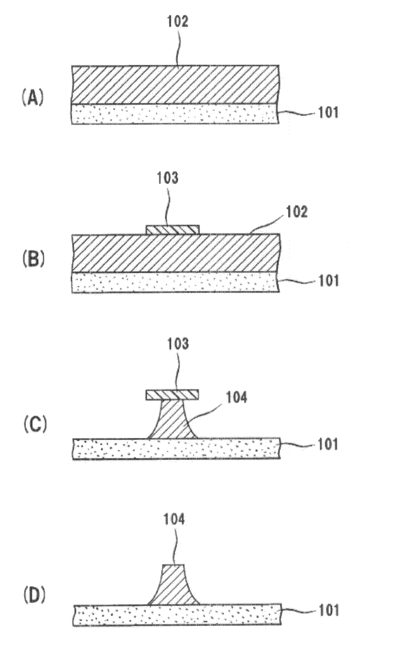
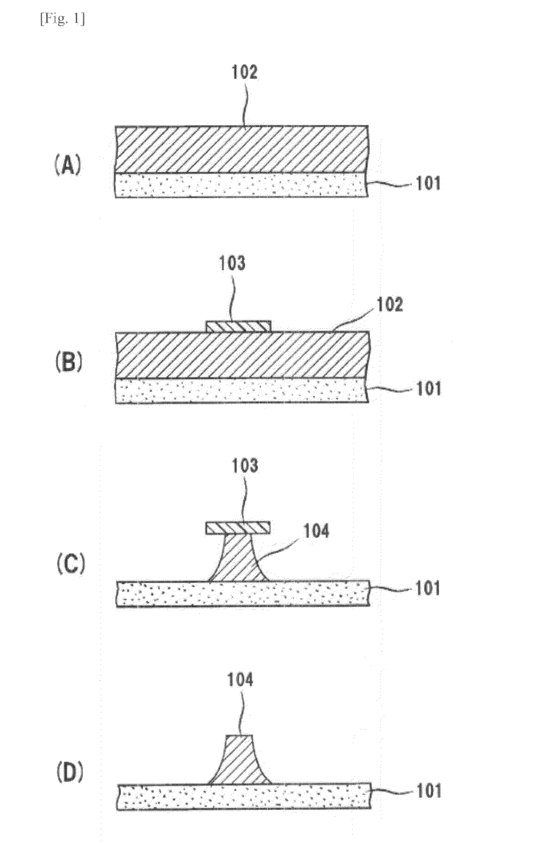
[0164]The photosensitive resist compositions A to K diluted with dipropylene glycol monomethyl ether to 400 dPa·s were each printed on a 1.6 mm-thick copper foil-etched substrate of glass epoxy (FR-4 substrate) and dried at 90° C. for 30 minutes, thereby obtaining substrates on which a resist having a dry film thickness of 300 μm or 400 μm was formed. Then, using an ultrahigh-pressure mercury lamp-equipped exposure apparatus (manufactured by ORC Manufacturing Co., Ltd.), a pattern having a minimum line-and-space of 300 μm was drawn on each of the thus obtained substrates at an ultraviolet exposure dose of 400 mJ / cm2. Thereafter, the pattern was developed with 30° C., 1 wt % aqueous sodium carbonate solution at a spray pressure of 2 atm and washed with water twice, thereby obtaining substrates having a photosensitive resist pattern formed thereon. The thus obtained substrates were cured in a hot-air drying oven at 150° C. for 1 hour.

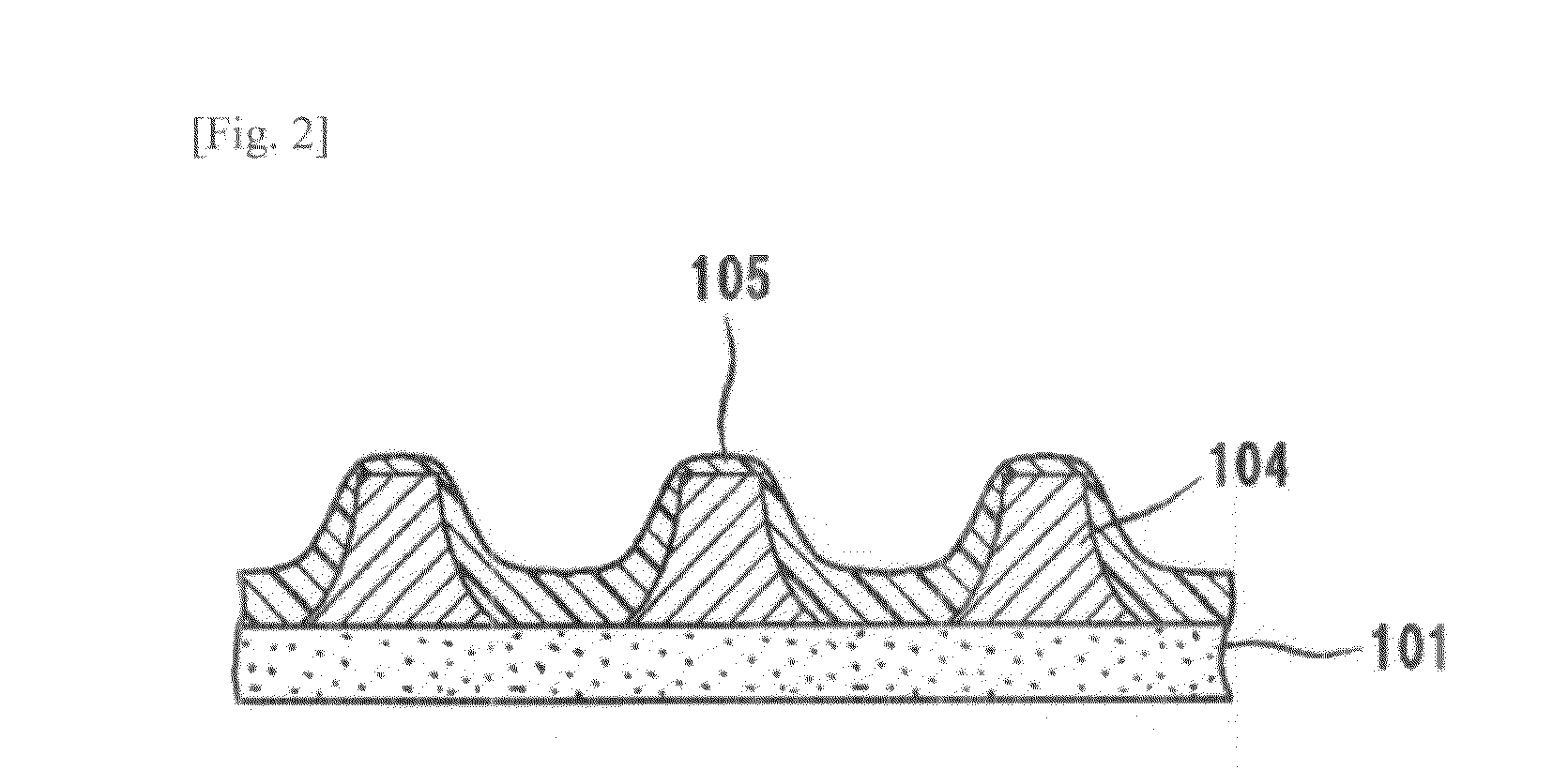
[0165]Next, on the entire surface of the thus obtai...

example 2

[0166]After subjecting each of the 300 μm-thick circuit substrates thus prepared with the photosensitive resists A to K in Example 1 to a CZ treatment using an apparatus manufactured by MEC COMPANY LTD., a prepreg (high-reliability glass epoxy multi-layer material R-1650C, manufactured by Panasonic Corporation) was pasted on both sides and the resultant was laminate-molded for 2 hours under heating conditions of 110° C.×30 minutes+180° C.×90 minutes, pressure conditions of 5 kgf / cm2×15 minutes+20 kgf / cm2 and a vacuum degree of 30 mmHg or less. The thus obtained 4-layer laminate was irradiated with single shot of carbon dioxide laser (output=13 mJ) to form a blind via-hole of 60 μm in diameter. Then, the photosensitive resists A to K having a dry film thickness of 300 μm were prepared under the above-described conditions and a circuit was formed therefrom in the same manner as in Example 1 to obtain a 4-layer circuit substrate having a minimum line-and-space of 300 μm. After subjecti...


PUM

PropertyMeasurementUnit
thicknessaaaaaaaaaa
thicknessaaaaaaaaaa
thicknessaaaaaaaaaa

Abstract

Provided is a photosensitive composition, which comprises a carboxyl group-containing resin, a photopolymerization initiator, a photosensitive acrylate compound and a filler, wherein the filler has a refractive index of 1.5 to 1.6 and a dry coating film of the photosensitive composition shows an absorbance of at least either 0.01 to 0.2 at a wavelength of 365 nm or 0.01 to 0.2 at a wavelength of 405 nm per thickness of 25 μm. The content of the filler is preferably 20 to 60 wt % with respect to the total amount of the composition. This photosensitive composition can be advantageously used as a plating resist of a printed wiring board or a solder resist and is useful particularly in the formation of a very finely patterned resist film having a high aspect ratio.

Description

TECHNICAL FIELD[0001]The present invention relates to a photosensitive composition, a cured coating film of the same and a printed wiring board of the same. More particularly, the present invention relates to a photosensitive composition which is required for producing a printed wiring board having a high aspect and a thick-film circuit pattern.BACKGROUND ART[0002]In printed wiring board for automobiles and high-power LED-equipped printed wiring boards, because of the necessity for allowing a large current to flow therethrough and the necessity for heat releasability, it is required that the circuit have a high aspect and be made thicker.[0003]Conventionally, as a method of forming a circuit pattern on a printed wiring board, a subtractive method is known. In this method, first, as shown in FIG. 1 (A), a photosensitive resin composition is coated and dried on a copper layer 102, which is formed on the surface of an insulating substrate 101. Then, the resultant is selectively exposed...

Claims


Application Information

Patent Timeline
Patent Type & Authority Applications(United States)
IPC IPC(8): G03F7/031H05K1/09H05K1/03G03F7/20
CPCG03F7/031H05K1/03H05K1/09G03F7/20G03F7/0047G03F7/027G03F7/032G03F7/033G03F7/035G03F7/038G03F7/0385H05K3/184H05K3/3452H05K2201/10106
Inventor IWAYAMA, GENTOARIMA, MASAO
Owner TAIYO INK MFG
Why Eureka
Try Eureka