Organic light emitting diode display device

a light-emitting diode and display device technology, applied in the direction of organic semiconductor devices, discharge tube luminescnet screens, test/measurement of semiconductor/solid-state devices, etc., can solve the problems of complex process for fabricating oled display devices, difficult to form projecting lenses for collecting light on the substrate, etc., to enhance light extraction efficiency and color reproducibility, improve brightness and color coordinate characteristics, simple structure and process

Active Publication Date: 2009-12-10
SAMSUNG DISPLAY CO LTD
View PDF12 Cites 54 Cited by
  • Summary
  • Abstract
  • Description
  • Claims
  • Application Information

AI Technical Summary

Benefits of technology

[0009]Aspects of the present invention provide an organic light emitting diode (OLED) display device which can improve brightness and color coordinate cha

Problems solved by technology

However, because a single pixel has a very small area, it is difficult to form the projecting lens for collecting

Method used


Image

  • Organic light emitting diode display device
  • Organic light emitting diode display device
  • Organic light emitting diode display device

Examples


experimental examples 1 to 4

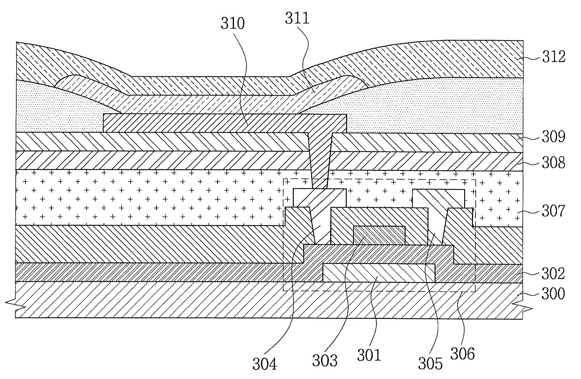
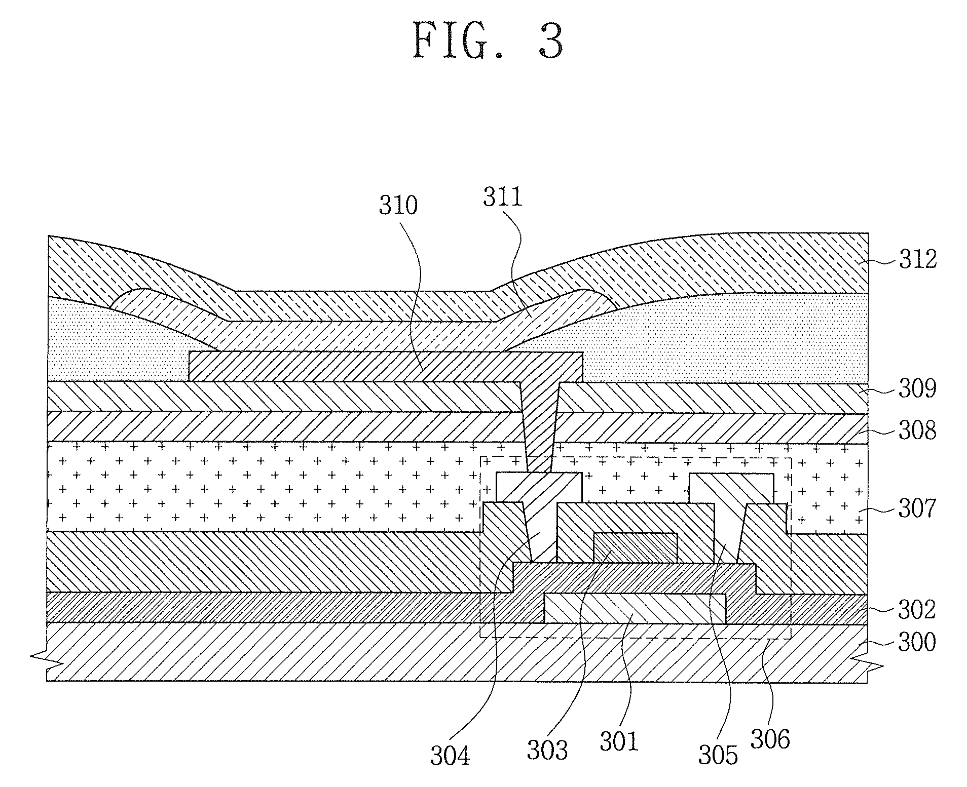
[0056]Sample OLED display devices were fabricated. Second refraction layers (Nb2O5, refractive index: 2.4) were formed to thicknesses listed in Table 1 on respective glass substrates. A first refraction layer (SiO2, refractive index: 1.45) was formed to a thickness of 30 nm on the second refraction layer. A first electrode, which was made of ITO, was formed to a thickness of 50 nm on the first refraction layer. A hole injection layer was formed to a thickness of 75 nm using DNTPD on the first electrode, and a hole transport layer was formed to a thickness of 15 nm using NPB on the hole injection layer. A blue emission layer was formed to a thickness of 25 nm using AND as a host and EK8 (Kodak) as a dopant on the hole transport layer. Subsequently, an electron transport layer was formed to a thickness of 25 nm using Alq3 on the blue emission layer, and an electron injection layer was formed to a thickness of 5 nm using LiF on the electron transport layer. A second electrode was forme...

experimental examples 5 to 8

[0057]Except that a first refraction layer was formed to a thickness of 90 nm, other sample OLED display devices were fabricated with the same conditions as in Experimental examples 1 to 4.

experimental examples 9 to 20

[0062]Second refraction layers (Nb2O5, refractive index: 2.4) were formed to thicknesses listed in Table 5 on respective glass substrates. A first refraction layer (SiO2, refractive index: 1.45) was formed to a thickness of 30 nm on the second refraction layer. The first electrode was formed to a thickness of 50 nm using ITO on the first refraction layer. Hole injection layers were formed to thicknesses of 145, 100 and 75 nm for red, green and blue pixels using DNTPD on the first electrode, respectively. A hole transport layer was formed to a thickness of 15 nm using NPB on the hole injection layers. A red emission layer was formed to a thickness of 45 nm using rubrene as a host and RD3 (Kodak) as a dopant, a green emission layer was formed to a thickness of 45 nm using Alq3 as a host and C545T as a dopant, and a blue emission layer was formed to a thickness of 25 nm using AND as a host and EK8 (Kodak) as a dopant on the hole transport layer. Subsequently, an electron transport laye...


PUM


Abstract

Provided is an organic light emitting diode display device which can improve brightness and color coordinate characteristics in all emission wavelength ranges, and thus can enhance light extraction efficiency and color reproducibility. The organic light emitting diode display device includes a substrate, a first electrode disposed on the substrate, an organic layer disposed on the first electrode and having an emission layer, a second electrode disposed on the organic layer, and first and second refraction layers. A stack of the first and second refraction layers is disposed either between the first electrode and the substrate or on the second electrode. A refractive index of the first refraction layer is smaller than a refractive index of the second refraction layer. A thickness of the first refraction layer is no greater than 100 nm.

Description

CLAIM OF PRIORITY[0001]This application makes reference to, incorporates the same herein, and claims all benefits accruing under 35 U.S.C. §119 from an application earlier filed in the Korean Intellectual Property Office on 5 Jun. 2008 and there duly assigned Serial No. 10-2008-0053339.BACKGROUND OF THE INVENTION[0002]1. Field of the Invention[0003]The present invention relates to an organic light emitting diode (OLED) display device, and more particularly, to an OLED display device which can improve brightness and color coordinate characteristics in all emission wavelength ranges using a simple structure and process and thus enhance light extraction efficiency and color reproducibility, by controlling thicknesses of first and second refraction layers disposed between an electrode and a transparent substrate.[0004]2. Description of the Related Art[0005]Light efficiency for light emitting devices, particularly flat panel display devices such as OLED display devices, is classified int...

Claims


Application Information

Patent Timeline
IPC IPC(8): H01J1/63
CPCH01L51/5265H01L2251/558H01L51/5275H10K50/852H10K50/858H10K2102/351H01L22/12
Inventor JUN, HYUK-SANGSONG, OK-KEUNJEONG, HYE-INKOO, YOUNG-MO
Owner SAMSUNG DISPLAY CO LTD
Why Eureka
Try Eureka