

Structure and Method of A Field-Enhanced Charge Trapping-DRAM
a charge trapping and charge technology, applied in the field of memory devices, can solve problems such as volatile memory, and achieve the effect of reducing operational voltage and increasing the operational speed of integrated circuit memory devices
- Summary
- Abstract
- Description
- Claims
- Application Information
AI Technical Summary
Benefits of technology
Problems solved by technology
Method used
Image

Examples
Embodiment Construction
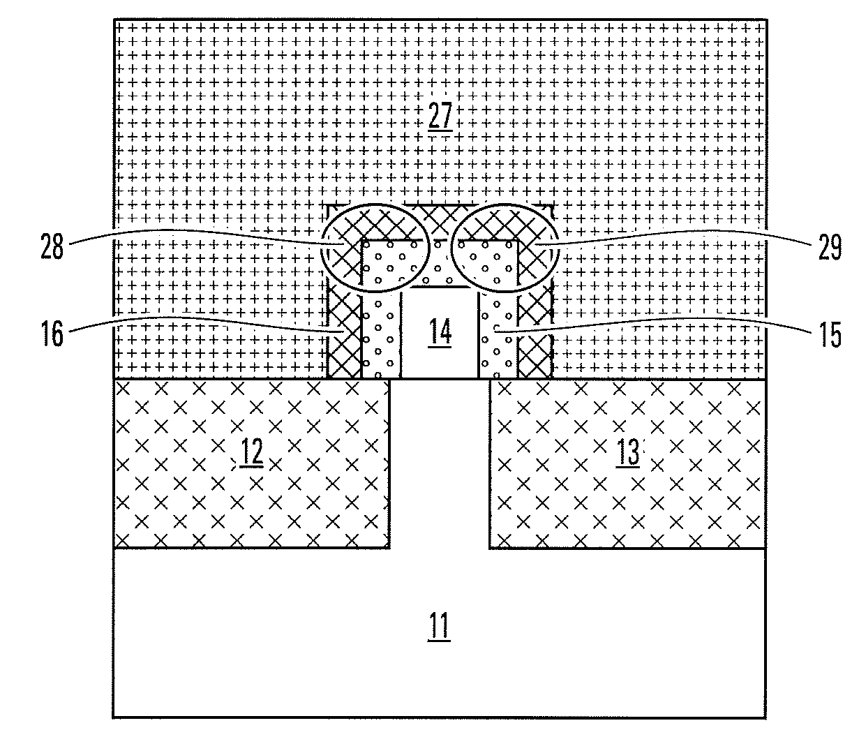
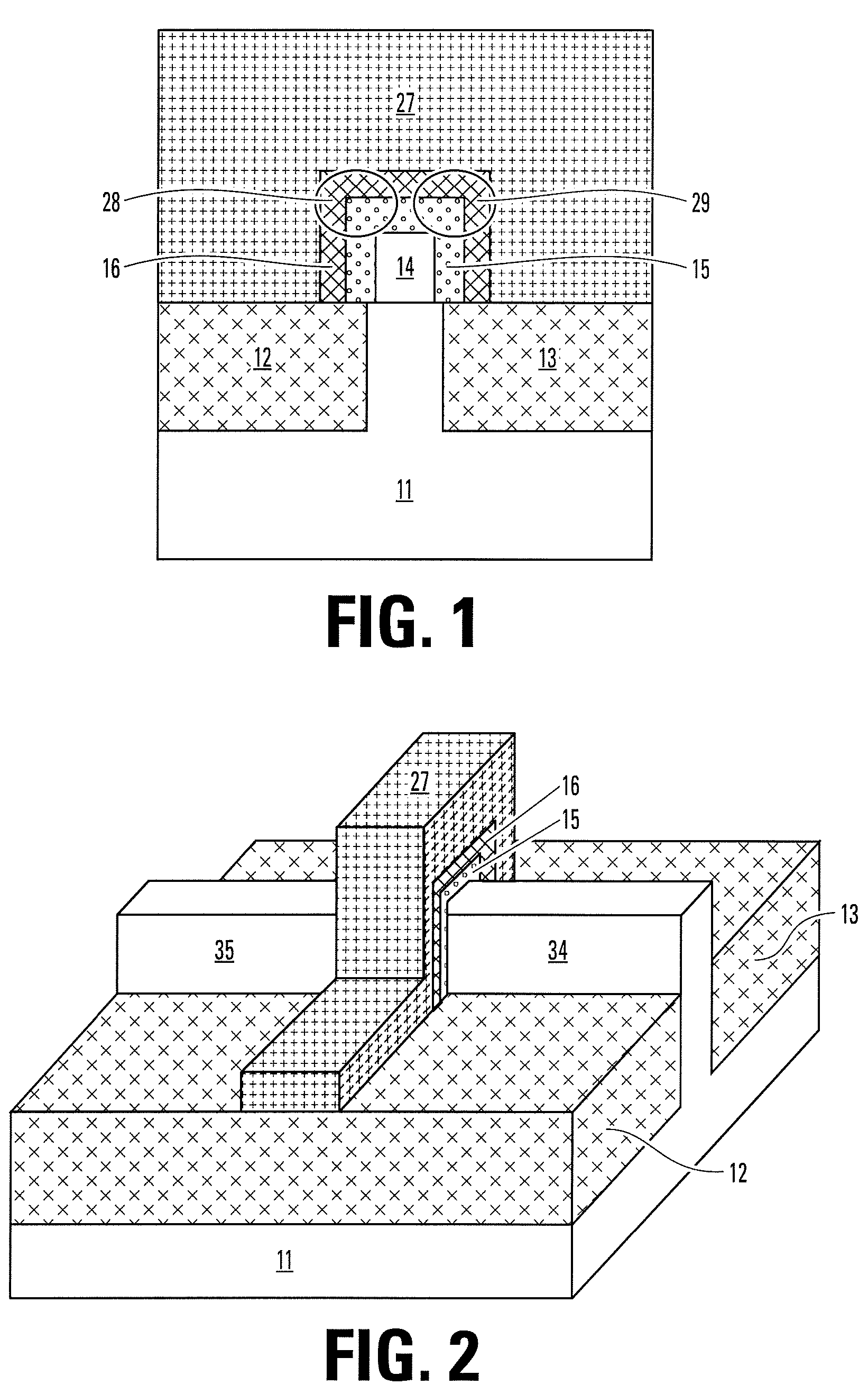
[0028]FIG. 1 illustrates a cross-sectional view of a FinFET-TDRAM memory structure with a PONIS (Poly / Oxide / Nitride / Si-substrate) structure. The memory is formed on a semiconductor substrate 11 (such as p-type silicon) with a first isolation oxide region 12 and a second isolation oxide region 13. A protruding semiconductor 14 of the memory extends from the semiconductor substrate 11, and is between the first isolation oxide 12 and the second isolation oxide 13. A volatile programmable structure 15 of the memory has an upside-down U-shape and covers the protruding semiconductor 14. The dielectric structure 16 also has an upside-down U-shape and covers the volatile programmable structure 15. A gate structure 27 covers the dielectric structure 16.
[0029]The bending parts of the volatile programmable structure 15 and the dielectric structure 16 form a first corner region 28 and a second corner region 29 in the volatile programmable structure. The first and second corner regions 28, 29 in...
PUM
 Abstract
Description
Claims
Application Information