Phosphorescent OLED device with mixed hosts

a phosphorescent el and host technology, applied in the direction of discharge tube/lamp details, discharge tube luminescnet screens, organic semiconductor devices, etc., can solve the problems of large efficiency loss, performance limitations, and many desirable applications, and achieve the effects of improving efficiency, driving voltage and operational stability, and improving luminan

Active Publication Date: 2009-12-17
GLOBAL OLED TECH
View PDF98 Cites 49 Cited by
  • Summary
  • Abstract
  • Description
  • Claims
  • Application Information

AI Technical Summary

Benefits of technology

[0016]The improvements found in devices of the invention include imp

Problems solved by technology

While organic electroluminescent (EL) devices have been known for over two decades, their performance limitations have represented a barrier to many desirable applications.
However, it is generally

Method used


Image

  • Phosphorescent OLED device with mixed hosts
  • Phosphorescent OLED device with mixed hosts
  • Phosphorescent OLED device with mixed hosts

Examples


examples

Device Examples 1-1 through 1-6

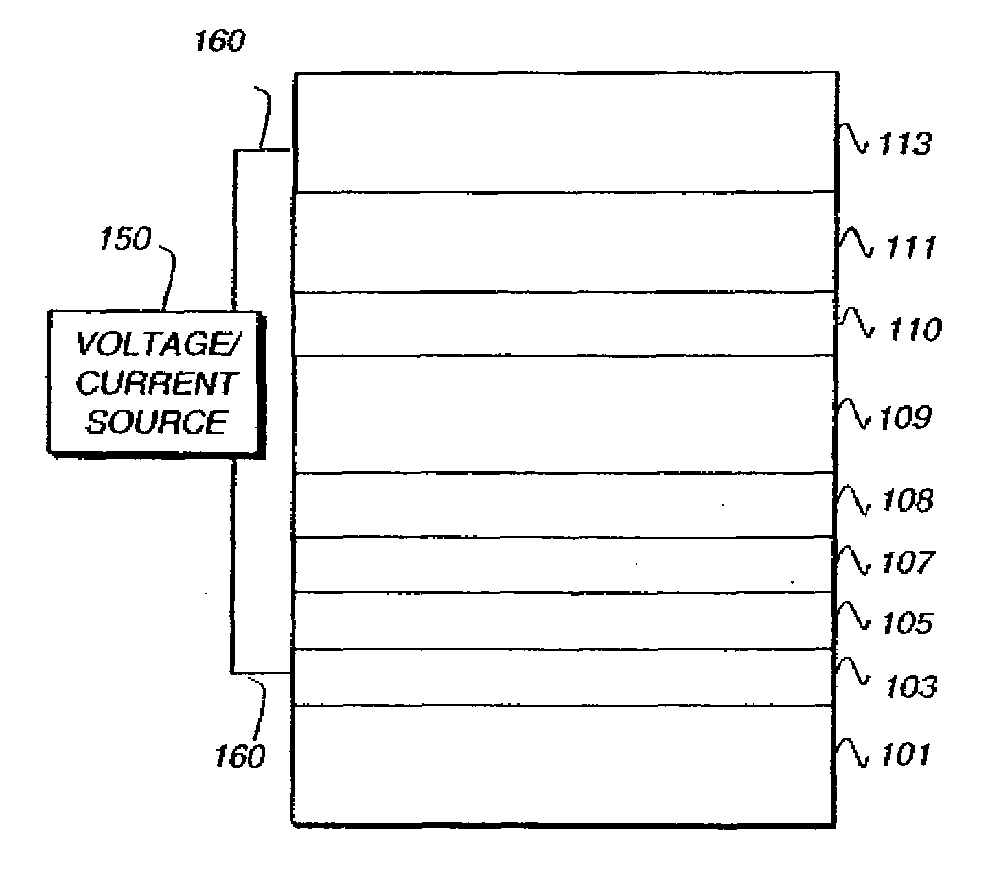
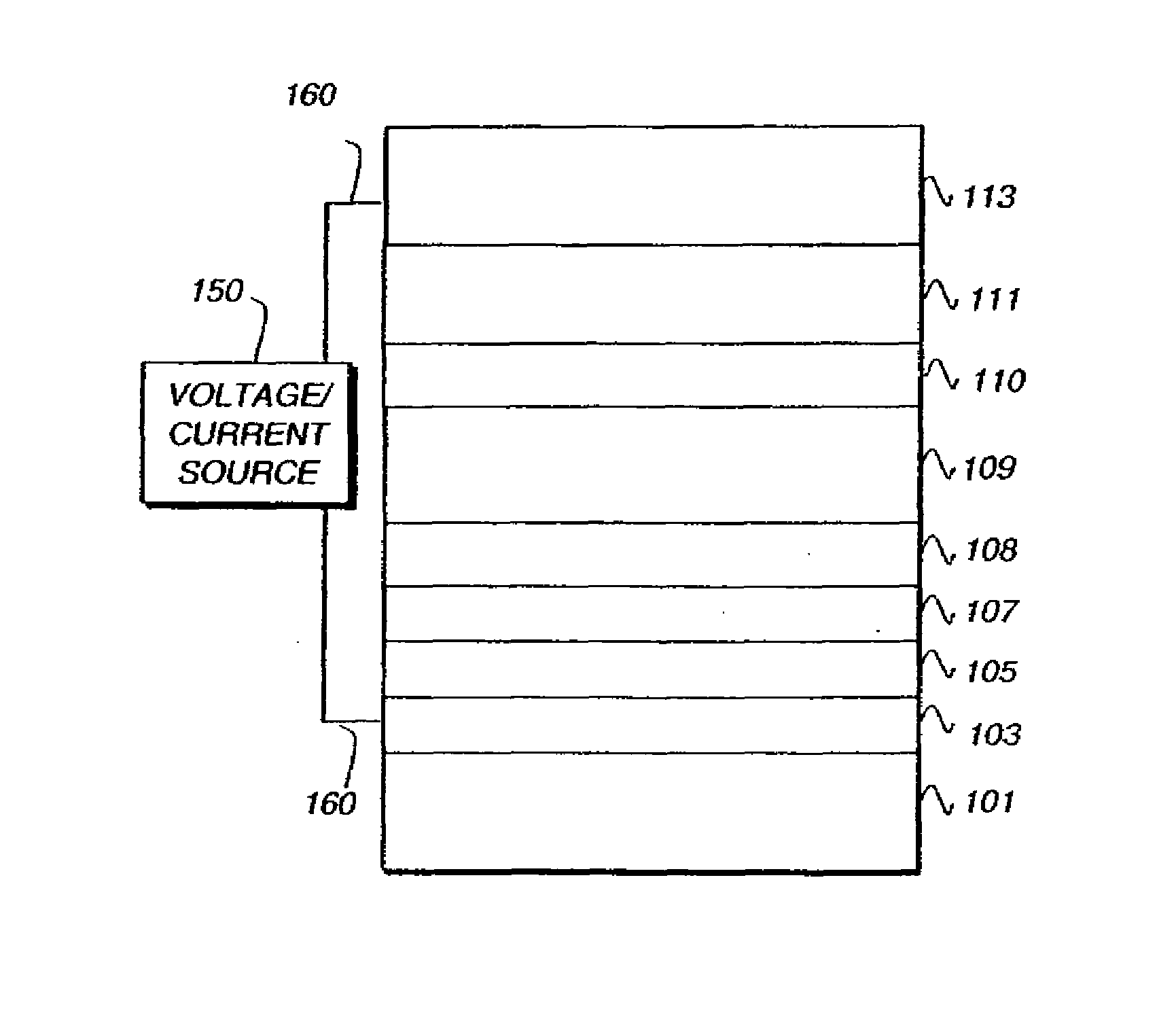
[0267]Inventive OLED devices were constructed in the following manner:[0268]1. A glass substrate, coated with an approximately 25 nm layer of indium-tin oxide (ITO) as the anode, was sequentially ultrasonicated in a commercial detergent, rinsed in deionized water, and exposed to an oxygen plasma for about 1 minute.[0269]2. Over the ITO a 1 nm fluorocarbon (CFx) hole injecting layer (HIL) was deposited by plasma-assisted deposition of CHF3 as described in U.S. Pat. No. 6,208,075.[0270]3. Next, a hole transporting layer (HTL) of NN′-di-1-naphthyl-N,N′-diphenyl-4,4′-diaminobiphenyl (NPB) was vacuum deposited to a thickness of 115 nm.[0271]4. A 35 nm light emitting layer (LEL) consisting of a mixture of GaC-1 as the electron transporting co-host, NPB as the hole transporting co-host, and fac-tris(1-phenyl-isoquinolinato-N̂C)Iridium(III) [i.e., Ir(1-piq)3] as a red phosphorescent emitter was then vacuum deposited onto the HTL. Concentration of NPB was vari...

examples 5-1 through 54

Device Examples 5-1 through 54

[0334]A comparative device 5-1 not satisfying the satisfying the requirements of the invention was fabricated in the following manner:[0335]1. A glass substrate, coated with an approximately 25 nm layer of indium-tin oxide (ITO) as the anode, was sequentially ultrasonicated in a commercial detergent, rinsed in deionized water, and exposed to an oxygen plasma for about 1 minute.[0336]2. Over the ITO a 1 nm fluorocarbon (CFx) hole injecting layer (HIL) was deposited by plasma-assisted deposition of CHF3 as described in U.S. Pat. No. 6,208,075.[0337]3. Next a HTL of NPB was vacuum deposited to a thickness of 95 nm.[0338]4. An exciton / electron blocking layer (EBL) of 4,4′,4″-tris(carbazolyl)-triphenylamine (TCTA) was vacuum deposited to a thickness of 10 nm.[0339]5. A 35 nm light emitting layer (LEL) consisting of a GaC-1 as host, and tris(2-phenyl-pyridinato-N,C2′)Iridium (III) [i.e., r(ppy)3] as a green phosphorescent emitter was then vacuum deposited ont...


PUM

PropertyMeasurementUnit
Fractionaaaaaaaaaa
Energyaaaaaaaaaa
Volumeaaaaaaaaaa

Abstract

An OLED device comprises a cathode, an anode, and has therebetween a light-emitting layer containing a phosphorescent emitter that emits yellow, orange or red light; a tertiary arylamine compound as a first host material, and a gallium complex with only nitrogen bidentate ligands as a second host material. Desirably, the phosphorescent emitter is an iridium complex.

Description

FIELD OF INVENTION[0001]This invention relates to organic electroluminescent (OLED) devices containing a yellow, orange or red light-emitting layer including a phosphorescent emitter and a mixture of particular gallium complexes and hole-transporting materials as hosts. More specifically, this invention relates to efficient and low voltage phosphorescent EL devices with improved operational stability.BACKGROUND OF THE INVENTION[0002]While organic electroluminescent (EL) devices have been known for over two decades, their performance limitations have represented a barrier to many desirable applications. In simplest form, an organic EL device is comprised of an anode for hole injection, a cathode for electron injection, and an organic medium sandwiched between these electrodes to support charge recombination that yields emission of light. These devices are also commonly referred to as organic light-emitting diodes, or OLEDs. Representative of earlier organic EL devices are Gurnee et a...

Claims


Application Information

Patent Timeline
IPC IPC(8): H01L51/52
CPCH01L51/0081H01L51/0082H01L51/0085H01L2251/5384H01L51/5048H01L51/5096H01L51/5016H10K85/326H10K85/324H10K85/342H10K50/11H10K2101/10H10K50/14H10K50/18H10K2101/90
Inventor ROYSTER, JR., TOMMIE L.KONDAKOVA, MARINA E.
Owner GLOBAL OLED TECH
Why Eureka
Try Eureka