Trench MOSFET with shallow trench structures

a technology of mosfet and trench structure, which is applied in the direction of basic electric elements, semiconductor devices, electrical equipment, etc., can solve the problems of shortening the contact between the epitaxial layer and the trench gate, and achieves the elimination of bv degradation in termination, the effect of reducing the amount of doping

Inactive Publication Date: 2009-12-24
FORCE MOS TECH CO LTD
View PDF5 Cites 40 Cited by
  • Summary
  • Abstract
  • Description
  • Claims
  • Application Information

AI Technical Summary

Benefits of technology

[0009]Another aspect of the present invention is that, in some preferred embodiments, the BV degradation in termination can be totally prevented without introducing the trench bottom Ion Implantation dopant into top surface of epitaxial layer by blocking the Ion Implantation with mask oxide used as hard mask for trench etching for trench gates. Meanwhile, no additional mask is required to achieve this structure because during the trench bottom Ion Implantation, the Ion is blocked by thick oxide covering top surface of epitaxial layer.
[0010]Another aspect of the present invention is that, in some preferred embodiments, terrace gates for gate connection is employed to avert shortage issue may caused by trench gate contacts penetrating trench gate bottoms.
[0011]Briefly, in a preferred embodiment as shown in FIG. 5, the present invention disclosed a trench MOSFET with shallow trench structure formed on a heavily doped substrate of a first semiconductor doping type (e.g., N type) coated with back metal (not shown) on rear side as drain. Onto said substrate, a lightly doped epitaxial layer of a same first semiconductor doping type is grown, and a plurality of trenches is etched wherein, especially, the trench for gate connection is wider than others. Doped poly is filled into said trenches with a gate insulation layer formed over the inner surface of said trenches to form trenched gates. A body region that is doped with a dopant of second conductivity type (e.g., P type), extends between every two adjacent trench gates. The bottom of each said trench is designed to be rounded and wrapped with a doping area which has same doping type and heavier doping concentration comparing to epitaxial layer and is marked as n* in FIG. 5. Source regions heavily doped with a first doping type (e.g., N type) are formed on top surface of the P body regions. Through a thick oxide layer deposited over epitaxial layer, source-body contact trenches and gate contact trenches are etched into epitaxial layer and trench gates for source-body connection and gate connection, respectively. At the bottom of each source-body contact trench, a contact area heavily doped with the second doping type ion (e.g., P type) is carried out, which will help to form a low-resistance contact between contact metal plug and said body region. Tungsten plugs acting as the contact metal are filled into those contact trenches to connect the source regions, the body regions and the trench gates to source metal and gate metal, respectively. Said gate metal also serves as metal field plate overlying P body and top surface of epitaxial layer with Ion Implantation dopant in termination. The metal field plate is beyond P body and overlap the epitaxial layer surface ranging from 2 to 10 um, which can alleviate the BV degradation caused by n* area on top surface of epitaxial layer in termination.

Problems solved by technology

On the other hand, if the trench depth is shallow, when etching the gate contact trench during fabricating process, it is possible to etch through doped polysilicon filled in gate trench and further penetrate through the gate oxide and result in a shortage of metal plug filled in trench gate contact to the epitaxial layer.

Method used


Image

  • Trench MOSFET with shallow trench structures
  • Trench MOSFET with shallow trench structures
  • Trench MOSFET with shallow trench structures

Examples


Embodiment Construction

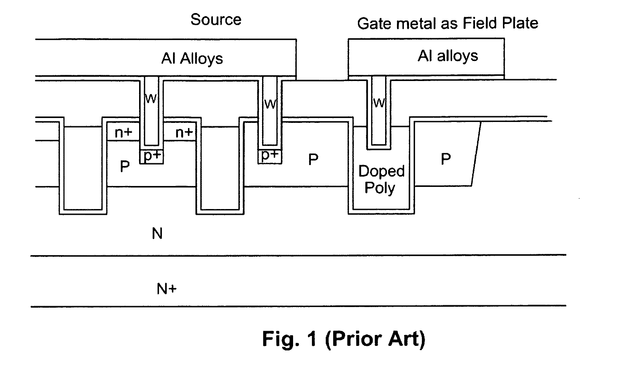
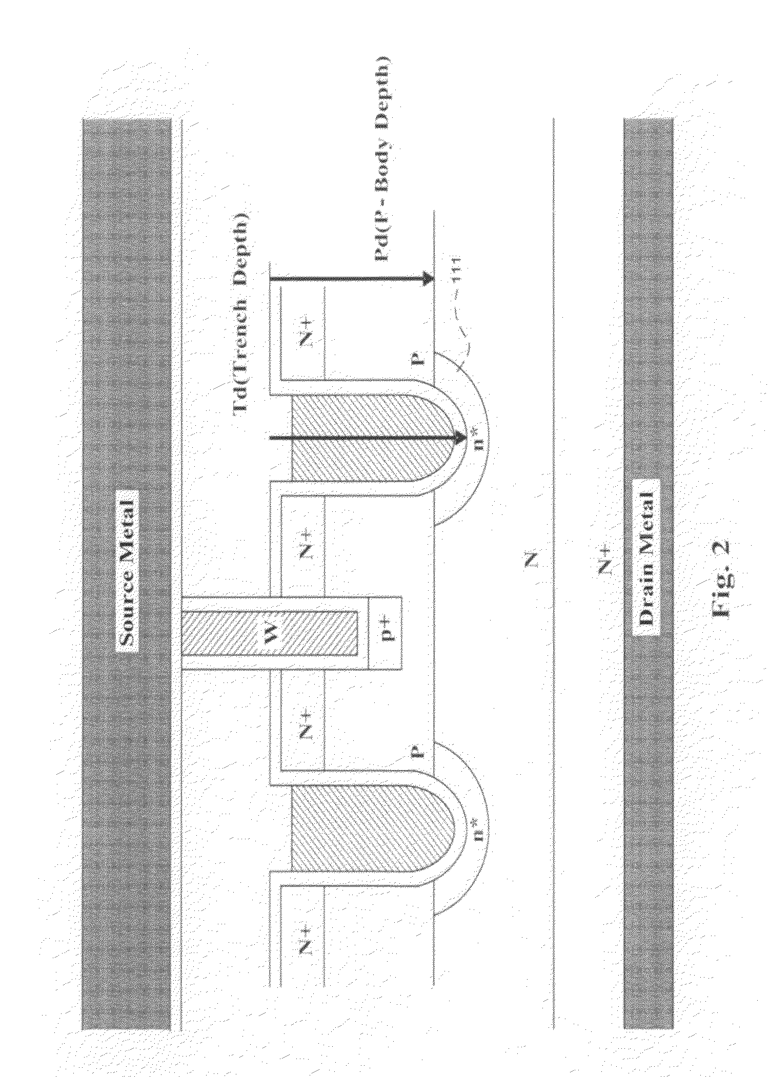
[0027]Please refer to FIG. 5 for a preferred embodiment of this invention where a trench MOSFET with shallow trench structure formed on a heavily N+ doped substrate 200 coated with back metal (not shown) on rear side as drain. Onto said substrate 200, a lightly N doped epitaxial layer 201 is grown, and a plurality of trenches is etched wherein. Doped poly is filled into said trenches with a gate insulation layer 220 formed over the inner surface of said trenches to form trenched gates 210 and at least a wider trench gate 211 for gate connection. A P body region 202 extends between said trench gates 210 and 211 with N+ source regions 203 near the top surface. The bottom of each trench is designed to be rounded and wrapped with an n* area 221 which has heavier doping concentration than the epitaxial layer 201. Trench source-body contacts filled with tungsten plug 212 is formed penetrating through a thick oxide layer 204 with contact p+implantation area 222 right below each source-body...


PUM


Abstract

A trench MOSFET with shallow trench structure is disclosed. The improved structure resolves the problem of degradation of BV caused by the As Ion Implantation in termination surface and no additional mask is needed which further enhance the avalanche capability and reduce the manufacture cost.

Description

CROSS REFERENCE TO RELATED APPLICATION[0001]This application is a continuation in part of U.S. patent application Ser. No. 12 / 143,714 filed on Jun. 20, 2008.BACKGROUND OF THE INVENTION[0002]1. Field of the Invention[0003]This invention relates generally to the cell configuration and fabrication process of trench MOSFET devices. More particularly, this invention relates to a novel and improved cell and termination structure, and improved process of fabricating a trench MOSFET with shallow trench structures having reduced drain-source resistance (Rds), and reduced gate charge (Qg), while maintaining a high Breakdown Voltage (BV).[0004]2. The Prior Arts[0005]Please refer to FIG. 1 for a trench MOSFET of prior art. In order to resolve the problem of high gate charge introduced in trench MOSFET of conventional configuration, shallow trench structures is disclosed by decreasing trench depth. However, the decrease in trench depth will lead to increase of Rds as shown in FIG. 3 (No As I / I c...

Claims


Application Information

Patent Timeline
Patent Type & Authority Applications(United States)
IPC IPC(8): H01L29/78H01L21/336
CPCH01L29/0878H01L29/402H01L29/41766H01L29/4236H01L29/42372H01L29/7813H01L29/456H01L29/4925H01L29/66727H01L29/66734H01L29/7811H01L29/42376H01L2224/06181
Inventor HSIEH, FU-YUAN
Owner FORCE MOS TECH CO LTD
Why Eureka
Try Eureka