Apparatus and method for inhibiting excess leakage current in unselected nonvolatile memory cells in an array

a non-volatile memory and array technology, applied in static storage, digital storage, instruments, etc., can solve the problems of increasing the number of its required external pins, bit line leakage current creating more of a problem, and the possibility of a read error or false read, so as to reduce the sub-threshold total leakage current

Inactive Publication Date: 2009-12-24
APLUS FLASH TECH
View PDF21 Cites 72 Cited by
  • Summary
  • Abstract
  • Description
  • Claims
  • Application Information

AI Technical Summary

Benefits of technology

[0019]An object of this invention is to provide an apparatus and method for reducing the sub-threshold total leakage current from all the

Problems solved by technology

One disadvantage of NOR flash nonvolatile memory is as the density is doubled, the number of its required external pin count increases by one due to the adding of one more external address pin.
The bit line leakage current creates more of a problem in program operations than read operations, because the program operation of the NOR-type flash nonvolatile memory cells requires a +5.0V bit line voltage to create a drain-to-source voltag

Method used


Image

  • Apparatus and method for inhibiting excess leakage current in unselected nonvolatile memory cells in an array
  • Apparatus and method for inhibiting excess leakage current in unselected nonvolatile memory cells in an array
  • Apparatus and method for inhibiting excess leakage current in unselected nonvolatile memory cells in an array

Examples


Embodiment Construction

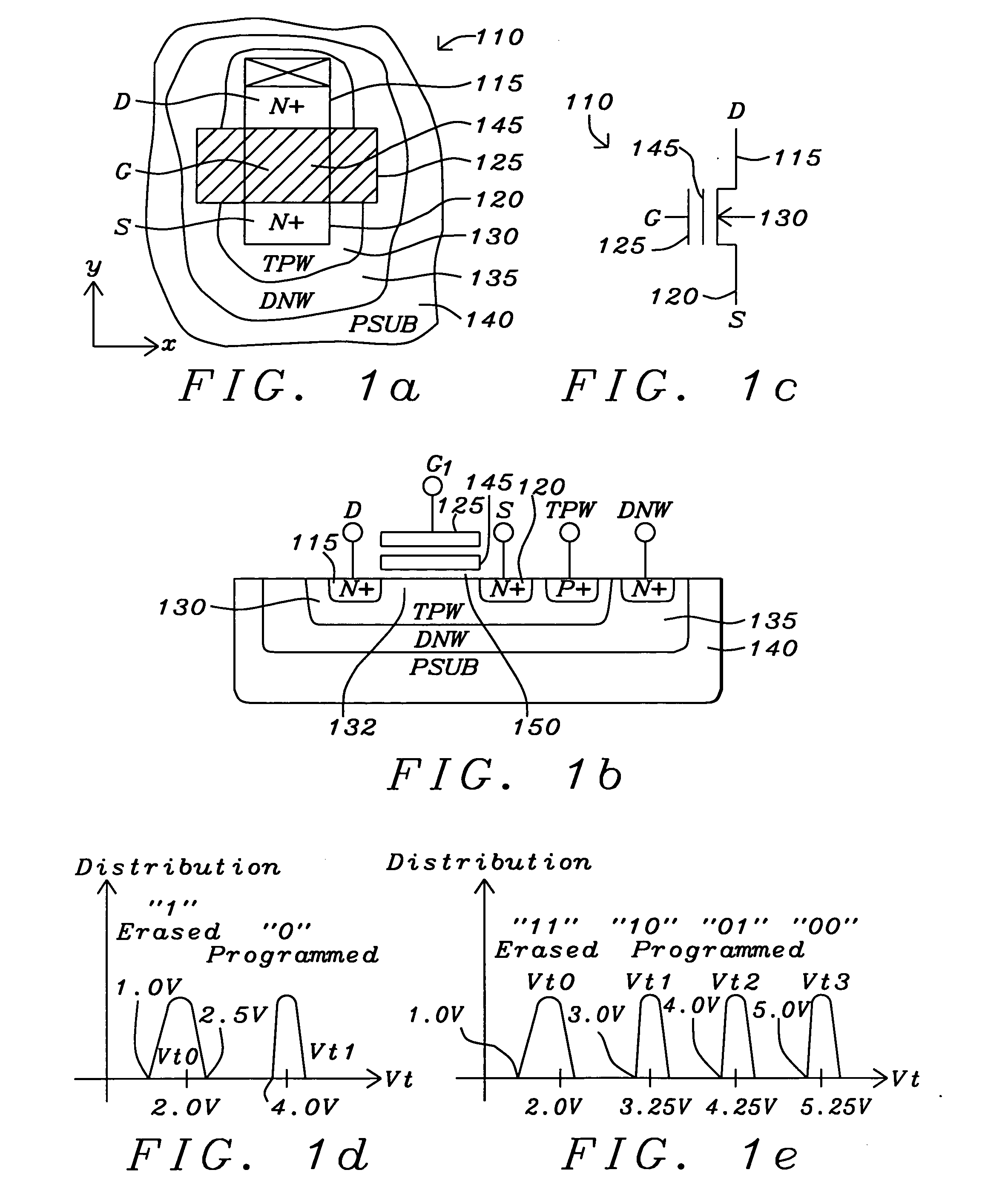
[0075]FIG. 1a is a top plan view of a NMOS NOR flash floating-gate transistor 110. FIG. 1b is a cross sectional view NMOS NOR flash floating-gate transistors 110FIG. 1c is the schematic symbol NMOS NOR flash floating-gate transistors 110. The floating-gate type NMOS NOR flash cell 110 is formed in the top surface of a triple P-type substrate 130. An N-type material is diffused into the surface of the P-type substrate 140 to form a deep N-well 135. A P-type material is then diffused into the surface of the deep N-well 135 to form a P-well 130 (commonly referred to as a triple P-well). The N-type material is then diffused into the surface of a P-type well 130 to form the drain (D) 115 and the self-aligned source (S) 120. A first polycrystalline silicon layer is formed above the bulk region of the P-type well 130 between the drain region 115 and the source region 120 to form the floating gate 145. A second polycrystalline silicon layer is formed over the floating gate 145 to create a c...


PUM


Abstract

An apparatus and method for operating an array of NOR connected flash nonvolatile memory cells erases the array in increments of a page, block, sector, or the entire array while minimizing sub-threshold leakage current through unselected nonvolatile memory cells. The apparatus has a row decoder circuit and a source decoder circuit for selecting the nonvolatile memory cells for providing biasing conditions for reading, programming, verifying, and erasing the selected nonvolatile memory cells while minimizing sub-threshold leakage current through unselected nonvolatile memory cells.

Description

[0001]This application claims priority under 35 U.S.C. §119 to U.S. Provisional Patent Application U.S. Patent Application Ser. No. 61 / 132,628, filed on Jun. 20, 2008, assigned to the same assignee as the present invention, and incorporated herein by reference in its entirety.RELATED PATENT APPLICATIONS[0002]U.S. patent application Ser. No. 12 / 387,771, filed on May 7, 2009.[0003]U.S. patent application Ser. No. 12 / 455,337, filed on Jun. 1, 2009 assigned to the same assignee as the present invention.[0004]Attorney Docket AP08-006, U.S. patent application Ser. No. ______, filed on ______.[0005]Attorney Docket AP08-007, U.S. patent application Ser. No. ______.BACKGROUND OF THE INVENTION[0006]1. Field of the Invention[0007]This invention relates generally to nonvolatile memory array structure and operation. More particularly, this invention relates to a NOR flash charge retaining nonvolatile memory device structures, peripheral circuits for NOR flash charge retaining nonvolatile memory ...

Claims


Application Information

Patent Timeline
IPC IPC(8): G11C16/06G11C16/04G11C7/00
CPCG11C11/5628G11C11/5635G11C11/5642G11C11/5671G11C2211/565G11C16/10G11C16/3436G11C2211/5621G11C2211/5641G11C16/0491
Inventor LEE, PETER WUNGHSU, FU-CHANGTSAO, HSING-YA
Owner APLUS FLASH TECH
Why Eureka
Try Eureka