
Microwave plasma processing apparatus

a processing apparatus and microwave technology, applied in the direction of chemical vapor deposition coating, coating, electric discharge tube, etc., can solve the problems of affecting the quality of microwave plasma processing equipmen

Inactive Publication Date: 2009-12-31
TOKYO ELECTRON LTD
View PDF4 Cites 158 Cited by
  • Summary
  • Abstract
  • Description
  • Claims
  • Application Information

AI Technical Summary

Problems solved by technology

Because a parallel plate or inductively-coupled high frequency plasma processing apparatus, which has been frequently used, has a high electron temperature, a deposited film or an underlying layer after plasma etching may be damaged.
Such damage may become a serious problem along with the miniaturization of the device elements.
In addition, while a gate insulator made of silicon oxynitride with better insulation properties has been considered as a substitute for a conventional thermally oxidized gate insulator with a decreasing thickness of a gate insulator, the silicon oxynitride film having sufficient insulation properties as the gate insulator cannot be provided by the conventional plasma processing apparatus because of plasma damage.

Method used


Image

  • Microwave plasma processing apparatus
  • Microwave plasma processing apparatus
  • Microwave plasma processing apparatus

Examples


first embodiment

A First Embodiment

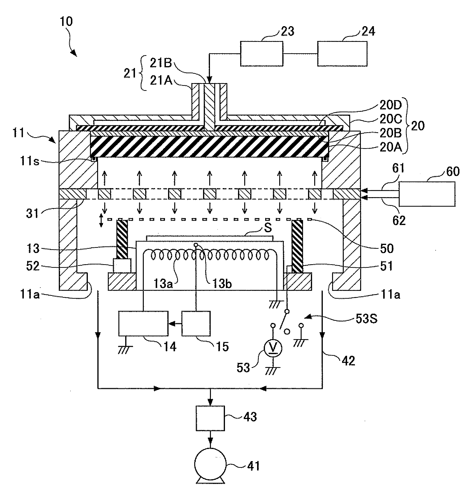
[0033]FIGS. 1A and 1B are schematic views illustrating a microwave plasma processing apparatus 10 according to a first embodiment of the present invention. The microwave plasma processing apparatus 10 according to this embodiment is configured as a plasma assisted film deposition apparatus where a silicon film such as an amorphous silicon film, a polycrystalline silicon film, or the like is deposited on a substrate.

[0034]Referring to FIG. 1A, the microwave plasma processing apparatus 10 includes a process chamber 11 and a susceptor 13 provided in the process chamber 11 in order to hold a substrate S by use of an electro-static chuck and the like.

[0035]The process chamber 11 may preferably be made of aluminum (Al), or austenitic stainless steel including Al. When the process chamber 11 is made of the austenitic stainless steel, a protection film of aluminum oxide is preferably formed on an inner wall surface by an oxidation treatment. A transfer opening (not shown) ...

second embodiment

A Second Embodiment

[0059]Next, a plasma processing apparatus according to a second embodiment of the present invention is explained. This plasma processing apparatus is different from the plasma processing apparatus 10 according to the first embodiment in that a temperature control system for controlling a temperature of the mesh plate 50 is provided. This plasma processing apparatus is mostly the same as the plasma processing apparatus 10 in other configurations. The following explanation focuses on the differences between this plasma processing apparatus and the plasma processing apparatus 10.

[0060]Referring to FIG. 3A, a plasma processing apparatus 200 according to the second embodiment of the present invention has a temperature control system 54. The temperature control system 54 has a heater 54a provided on the mesh plate 50, an electric power source 54b that supplies electricity to the heater 54a, a thermocouple 54c that extends to the mesh plate 50 through the supporting memb...

third embodiment

A Third Embodiment

[0063]Next, a plasma processing apparatus according to a third embodiment of the present invention is explained. FIG. 4 is a schematic view illustrating a plasma processing apparatus 300 according to the third embodiment of the present invention. As is understood by comparing FIG. 4 with FIG. 1, the plasma processing apparatus 300 according to the third embodiment is different from the plasma processing apparatus 10 according to the first embodiment in terms of a configuration of a gas supplying portion (e.g., the shower plate) and a positional relationship between the gas supplying portion and the mesh plate 50. This plasma processing apparatus 300 is mostly the same as the plasma processing apparatus 10 in other configurations. The following explanation focuses on the differences between this plasma processing apparatus 200 and the plasma processing apparatus 10 of the other configurations.

[0064]Referring to FIG. 4, the plasma processing apparatus 300 has a showe...


PUM

PropertyMeasurementUnit
Temperatureaaaaaaaaaa
Pressureaaaaaaaaaa
Electric potential / voltageaaaaaaaaaa

Abstract

A disclosed microwave plasma processing apparatus includes a process chamber whose inside may be maintained at a reduced pressure; a susceptor that is provided in the process chamber and holds a substrate; a gas supplying portion configured to supply a gas to the process chamber; a microwave generating portion that generates microwaves; a plasma introducing portion that is arranged to oppose the susceptor and introduces the microwaves generated by the microwave generating portion to the process chamber; and a mesh member arranged between the plasma introducing portion and the susceptor.

Description

BACKGROUND OF THE INVENTION[0001]1. Field of the Invention[0002]The present invention relates to a microwave plasma processing apparatus where plasma is generated by microwaves in a process chamber and a substrate held inside the process chamber is processed by use of the plasma.[0003]2. Description of the Related Art[0004]Plasma process technology is essential for a semiconductor device fabrication process. In recent years, miniaturization of device elements has been promoted from a demand for highly-integrated large scale integration (LSI) circuits. Along with this, a plasma processing apparatus suitable for such miniaturization is also in high demand. Because a parallel plate or inductively-coupled high frequency plasma processing apparatus, which has been frequently used, has a high electron temperature, a deposited film or an underlying layer after plasma etching may be damaged. Such damage may become a serious problem along with the miniaturization of the device elements. In a...

Claims


Application Information

Patent Timeline
IPC IPC(8): C23C16/54
CPCH01J37/32192H01J37/3244H01J37/32697H01J37/32623H01J37/32522
Inventor TANAKA, KOUJI
Owner TOKYO ELECTRON LTD
Features
  • Generate Ideas
  • Intellectual Property
  • Life Sciences
  • Materials
  • Tech Scout
  • Unparalleled Data Quality
  • Higher Quality Content
  • 60% Fewer Hallucinations
Learn More