

Electrical inspection substrate unit and manufacturing method therefore
a technology of substrate unit and electric inspection, which is applied in the direction of conductive pattern formation, instruments, chemistry apparatus and processes, etc., can solve the problems of no attempt to develop a low-temperature-firable ceramic composition which exhibits low thermal expansion, and achieves enhanced electrical reliability, enhanced mechanical strength, and convenient operation
Active Publication Date: 2009-12-31
NGK SPARK PLUG CO LTD
View PDF5 Cites 25 Cited by
- Summary
- Abstract
- Description
- Claims
- Application Information
AI Technical Summary
Benefits of technology
[0029]The borosilicate glass may further contain Li2O, which is an alkali metal oxide, in an amount of 0.1 mass % or less. When the amount of Li2O contained in the borosilicate glass is 0.1 mass % or less, migration of Ag (i.e., a conductive component) is less likely to occur, and, therefore, electrical reliability is enhanced.
[0030]Still further, the amount of mullite may be 20 vol. % to 45 vol. % (preferably 35 vol. % to 45 vol. %) on the basis of the entirety
Problems solved by technology
Despite the aforementioned conventional partial attempts, no attempts have been made to develop a low-temperature-firable ceramic composition which exhibits low thermal expansion and which is suitable for use in a const
Method used
View moreImage
Smart ImageViewing Examples

Examples
 PUM
| Property | Measurement | Unit |
|---|---|---|
| Temperature | aaaaa | aaaaa |
| Temperature | aaaaa | aaaaa |
| Percent by mass | aaaaa | aaaaa |
Abstract
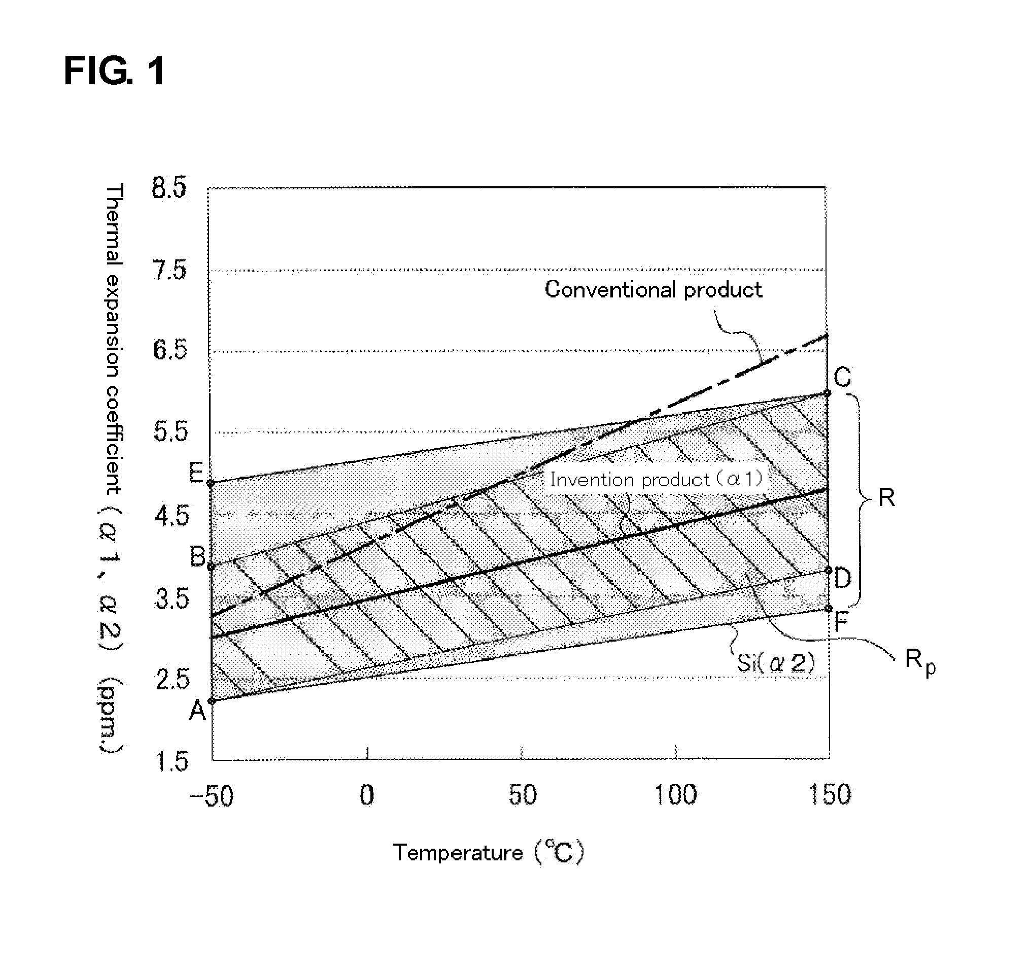
An electrical testing substrate unit includes a multi-layer ceramic substrate formed of mullite and a borosilicate glass as predominant ceramic components. In the multi-layer ceramic substrate, the borosilicate glass contains an alkali metal oxide in an amount of 0.5 to 1.5 mass %. The multi-layer ceramic substrate has a mean coefficient of linear thermal expansion having a value of 3.0 to 4.0 ppm/° C. between −50° C. and 150° C. A thermal expansion coefficient, α1, of the multi-layer ceramic substrate as determined at a particular temperature and a thermal expansion coefficient, α2, of a to-be-tested silicon wafer as determined at the same temperature silicon satisfy a relation: 0 ppm/° C.<α1−α2≦2.5 ppm/° C. through the temperature range of −50° C. to 150° C. Electrodes are formed on a surface of the multi-layer ceramic substrate.
Description
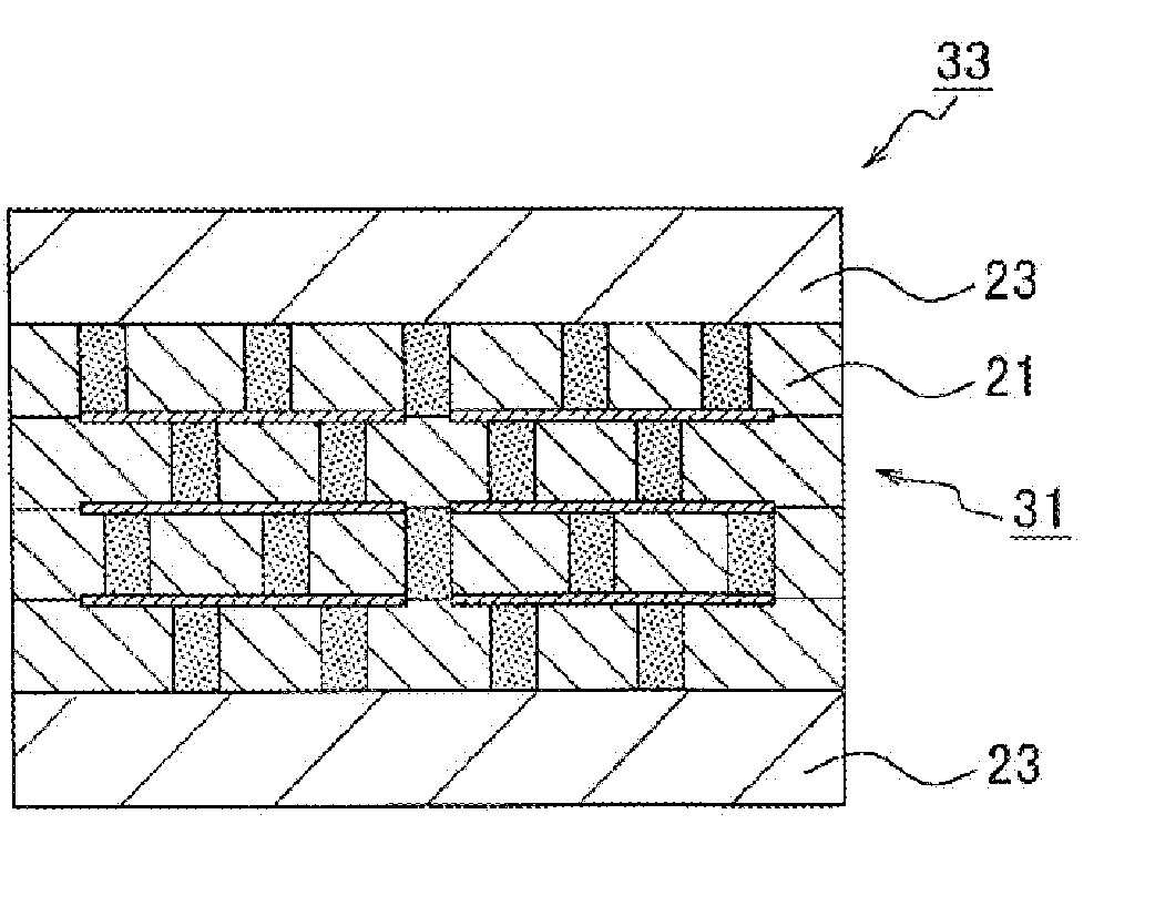
CROSS-REFERENCE TO RELATED APPLICATIONS[0001]This application is based on and claims priority to Japanese patent Application No. 2008-170737 filed Jun. 30, 2008 and Japanese patent Application No. 2009-102147 filed Apr. 20, 2009, the above applications incorporated herein by reference in their entirety.BACKGROUND OF THE INVENTION[0002]1. Field of the Invention[0003]The present invention relates to an electrical inspection substrate unit including a multi-layer ceramic substrate which realizes highly accurate mounting, on a surface layer thereof, of connecting terminals for electrical inspection of a silicon wafer, and which can expand or shrink in a manner similar to that of a silicon wafer having a circuit thereon, even in the case where inspection is conducted over a wide temperature range (−50° C. to 150° C.).[0004]2. Description of Related Art[0005]In recent years, in IC chip inspections, the inspections performed on a silicon wafer unit have been required frequently. Particular...
Claims
Login to View More Application Information
Patent Timeline
 IPC IPC(8): H05K1/02B32B37/06
CPCG01R1/0491G01R3/00G01R31/2863H05K1/0306H05K1/113Y10T29/49155H05K3/4611H05K3/4629H05K2201/0347H05K2203/025H05K2203/308H05K3/388
InventorTAKAHASHI, HIROYUKIHONDA, CHIEKATO, TATSUYAYAMADA, TOMOHIDETAGA, SHIGERU
OwnerNGK SPARK PLUG CO LTD