

Waveguide photodetector
a waveguide and photodetector technology, applied in the field of waveguide photodetectors, can solve the problems of increasing device capacitance, waveguide photodetectors with low reliability, and degrading or destroying photodetectors, and achieve the effect of high reliability and high speed respons
- Summary
- Abstract
- Description
- Claims
- Application Information
AI Technical Summary
Benefits of technology
Problems solved by technology
Method used
Image

Examples
first embodiment
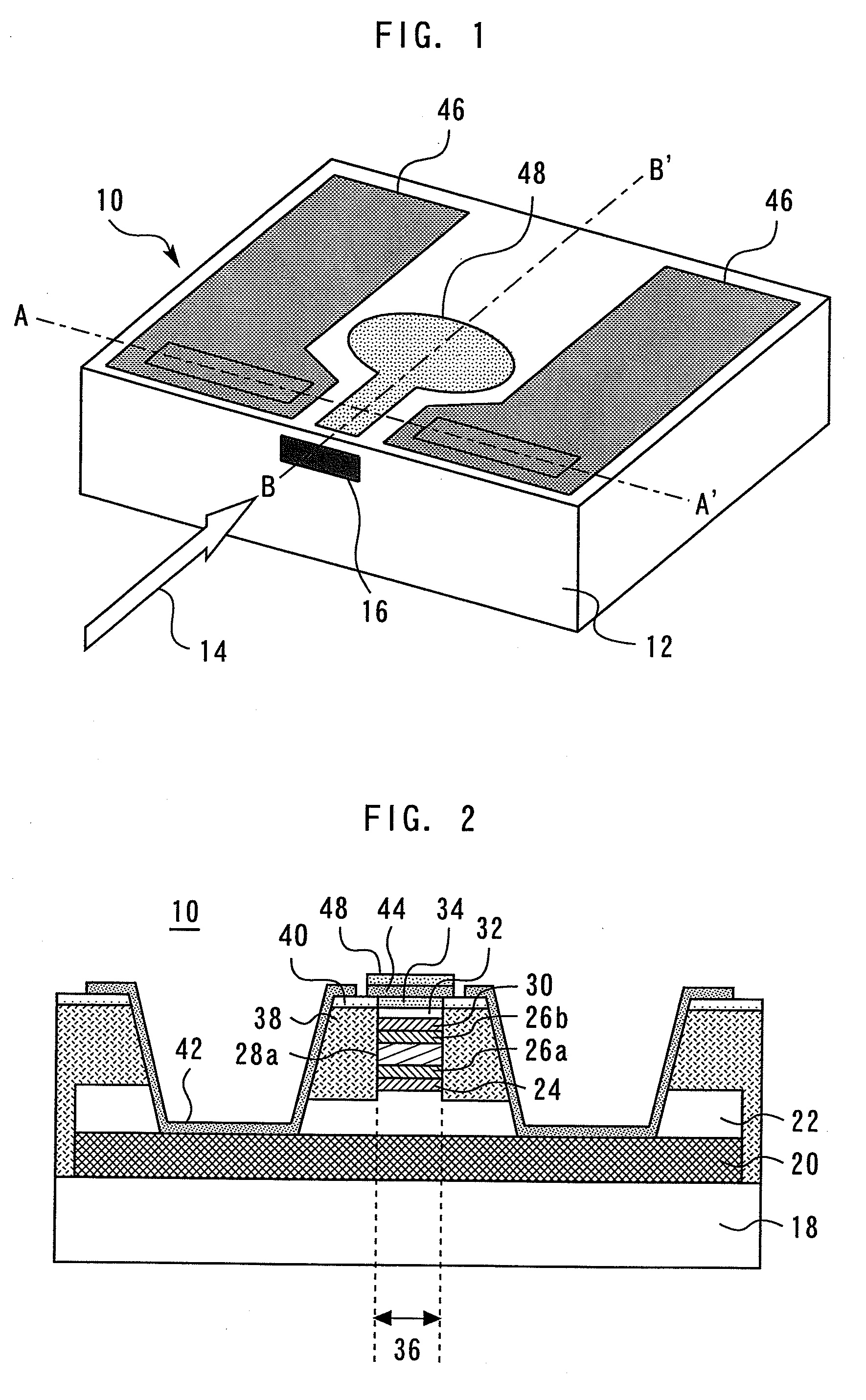
[0020]FIG. 1 is a perspective view of a waveguide photodetector 10 according to a first embodiment of the present invention. Light 14 incident on the light receiving end face 12 of the waveguide photodetector 10 propagates through a waveguide 16 toward the other end of the photodetector while being progressively absorbed in the waveguide.
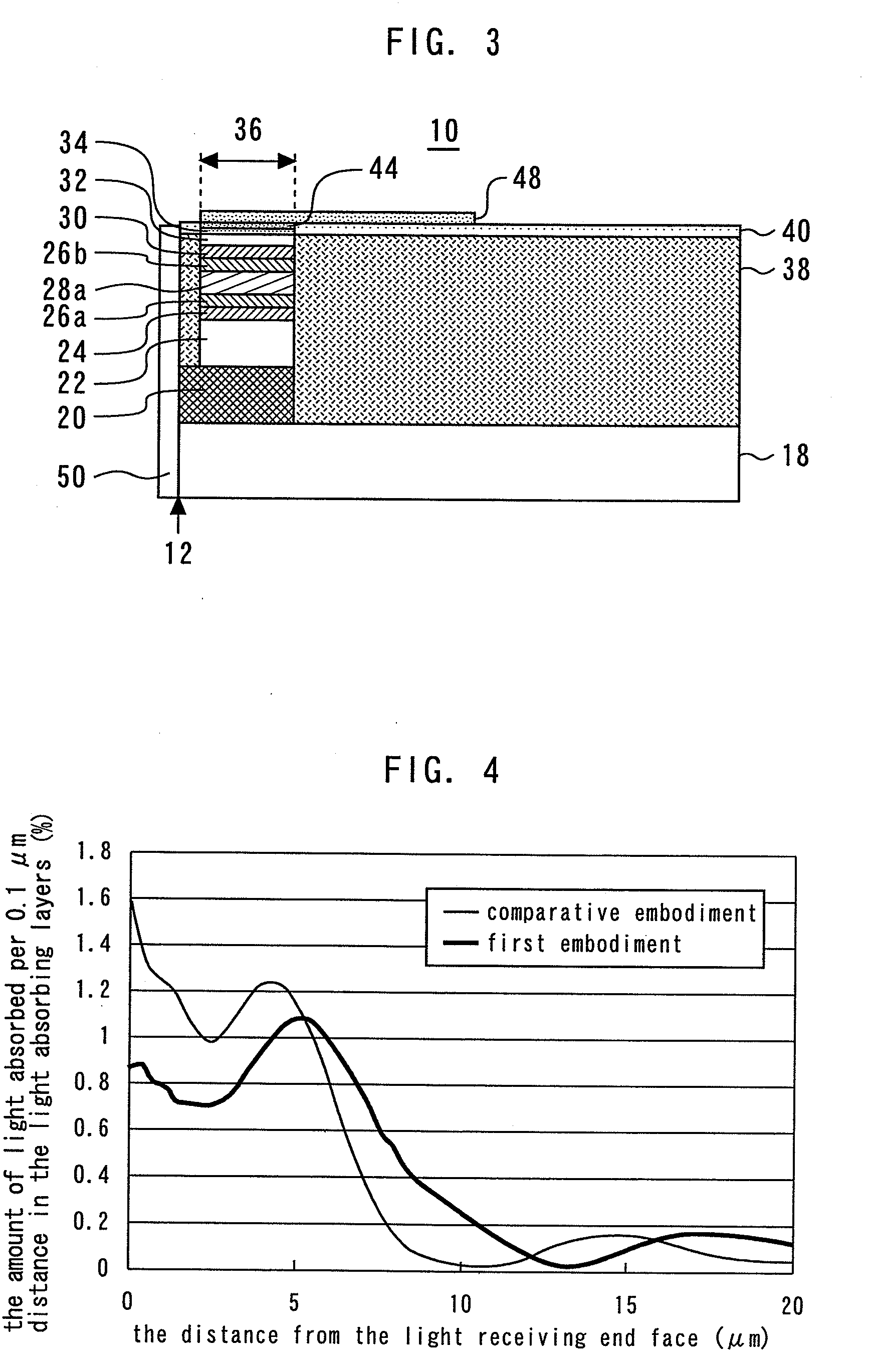
[0021]FIG. 2 is a cross-sectional view taken along line A-A′ of FIG. 1, and FIG. 3 is a cross-sectional view taken along line B-B′ of FIG. 1. Referring to FIGS. 2 and 3, the waveguide photodetector 10 includes a layer stack structure (or laminated structure) formed on a semi-insulating Fe—InP substrate 18. The layer stack structure includes an n-InGaAs contact layer 20, an n-InP cladding layer 22, an n-InGaAsP guiding layer 24 (having a composition for providing a wavelength of 1.4 μm), an i-InGaAs light absorbing layer 26a (0.15 μm thick), an i-InGaAsP non-light-absorbing layer 28a (0.2 μm thick), an i-InGaAs light absorbing layer 26b (0.15 μm thic...
second embodiment
[0029]FIGS. 6 and 7 show, in cross-section, a waveguide photodetector according to a second embodiment of the present invention. The perspective view of FIG. 1 also applies to this waveguide photodetector. That is, FIG. 6 is a cross-sectional view of the photodetector taken along line A-A′ of FIG. 1, and FIG. 7 is a cross-sectional view taken along line B-B′ of FIG. 1.
[0030]The waveguide photodetector of the present embodiment differs from that of the first embodiment in that it includes, as undoped semiconductor layers, an i-InGaAs light absorbing layer 26c (0.05 μm thick), an i-InGaAsP non-light-absorbing layer 28b (0.15 μm thick), an i-InGaAs light absorbing layer 26d (0.1 μm thick), an i-InGaAsP non-light-absorbing layer 28c (0.15 μm thick), and an i-InGaAs light absorbing layer 26e (0.05 μm thick) formed on top of one another in that order, instead of the i-InGaAs light absorbing layers 26a and 26b and the i-InGaAsP non-light-absorbing layer 28a. All other components are the sa...
third embodiment
[0033]FIGS. 10 and 11 show, in cross-section, a waveguide photodetector according to a third embodiment of the present invention. The perspective view of FIG. 1 also applies to this waveguide photodetector. That is, FIG. 10 is a cross-sectional view of the photodetector taken along line A-A′ of FIG. 1, and FIG. 11 is a cross-sectional view taken along line B-B′ of FIG. 1.
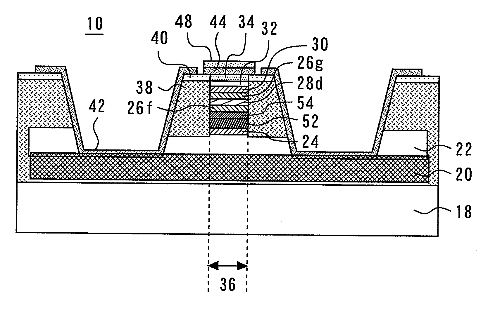
[0034]The waveguide photodetector of the present embodiment differs from that of the first embodiment in that it includes an i-AlInAs multiplication layer 52, a p-AlInAs electric field reduction layer 54, an i-InGaAs light absorbing layer 26f (0.15 μm thick), an i-InGaAsP non-light-absorbing layer 28d (0.2 μm thick), and an i-InGaAs light absorbing layer 26g (0.15 μm thick) formed on top of one another in that order, instead of the i-InGaAs light absorbing layers 26a and 26b and the i-InGaAsP non-light-absorbing layer 28a. All other components are the same as in the first embodiment.
[0035]Thus the waveguide photodet...
PUM
 Abstract
Description
Claims
Application Information