Through-substrate vias and method of fabricating same

Inactive Publication Date: 2010-01-07
TELEDYNE SCI & IMAGING
View PDF19 Cites 36 Cited by
  • Summary
  • Abstract
  • Description
  • Claims
  • Application Information

AI Technical Summary

Benefits of technology

[0012]The present method may be successfully practiced at temperatures of less than 200° C., thereby avoiding damage to circuitry residing on the substrate that might

Problems solved by technology

However, planar chip designs limit the amount of circuitry that can be placed on a single substrate.
Although three-dimensional chips using through-substrate vias have proven useful, they are currently limited.
Although this approach provides some advantages, it introduces other limitations, such as the inability to fabricate small-diameter, fine-pitch vias.
This limits the etch depth of the vias, and also reduces the amount of available space on the substrate for other uses.
Both dry etching and wet etching have been demonstrated for the thick wafer processing, and both suffer from constraints on via size and separation.
In addition, it is very difficult to reliably deposit electrical isolation layers and metallic conductors using low process temperatures in high aspect ratio vias.
This approach can use well-developed fabrication processes; however, disadvantages arise from the need for sequential processing of each successive layer and the complexity of intermediate testing.
Further, the thinning of the stacked wafers reduces their integrity an

Method used


Image

  • Through-substrate vias and method of fabricating same
  • Through-substrate vias and method of fabricating same
  • Through-substrate vias and method of fabricating same

Examples


Example

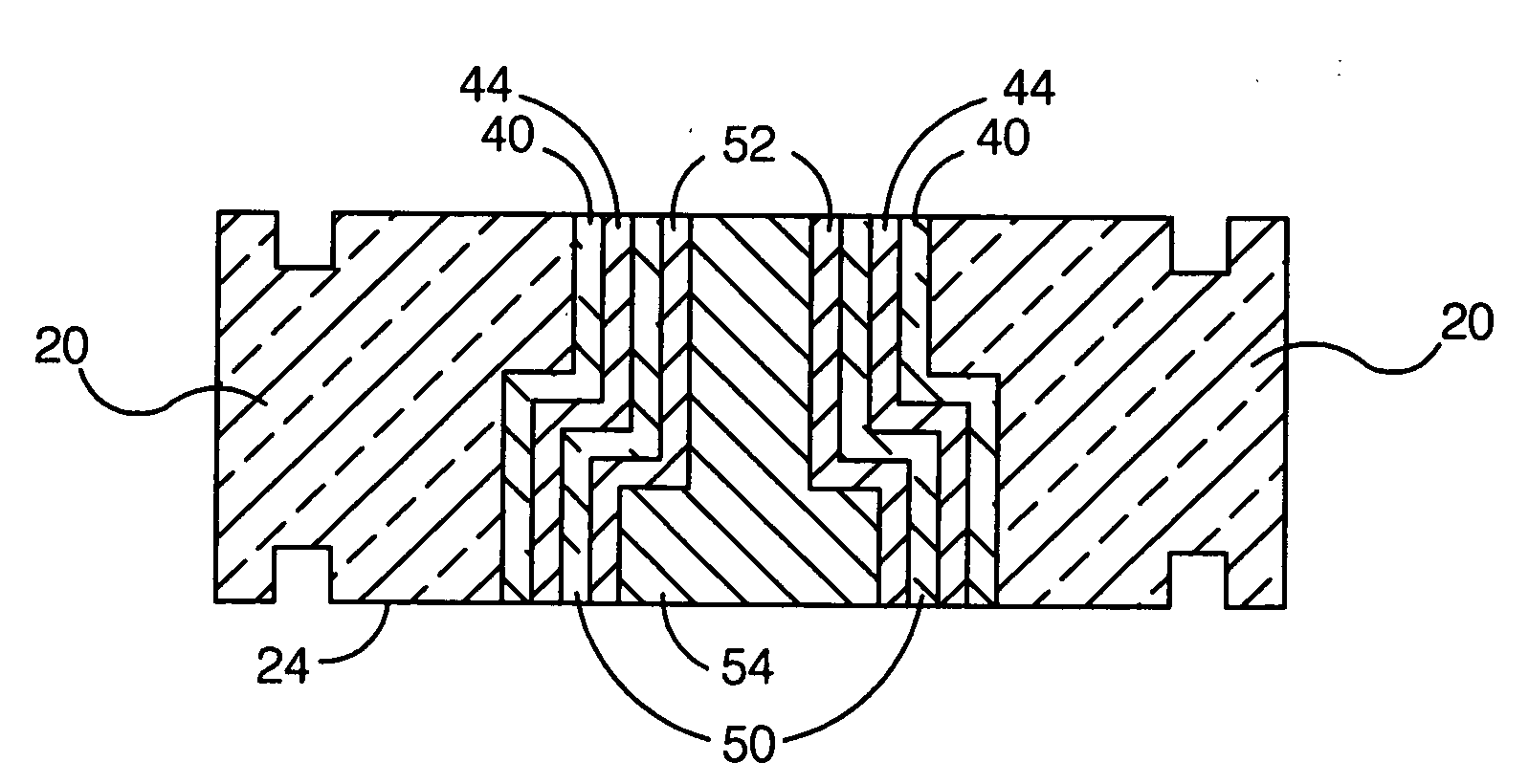
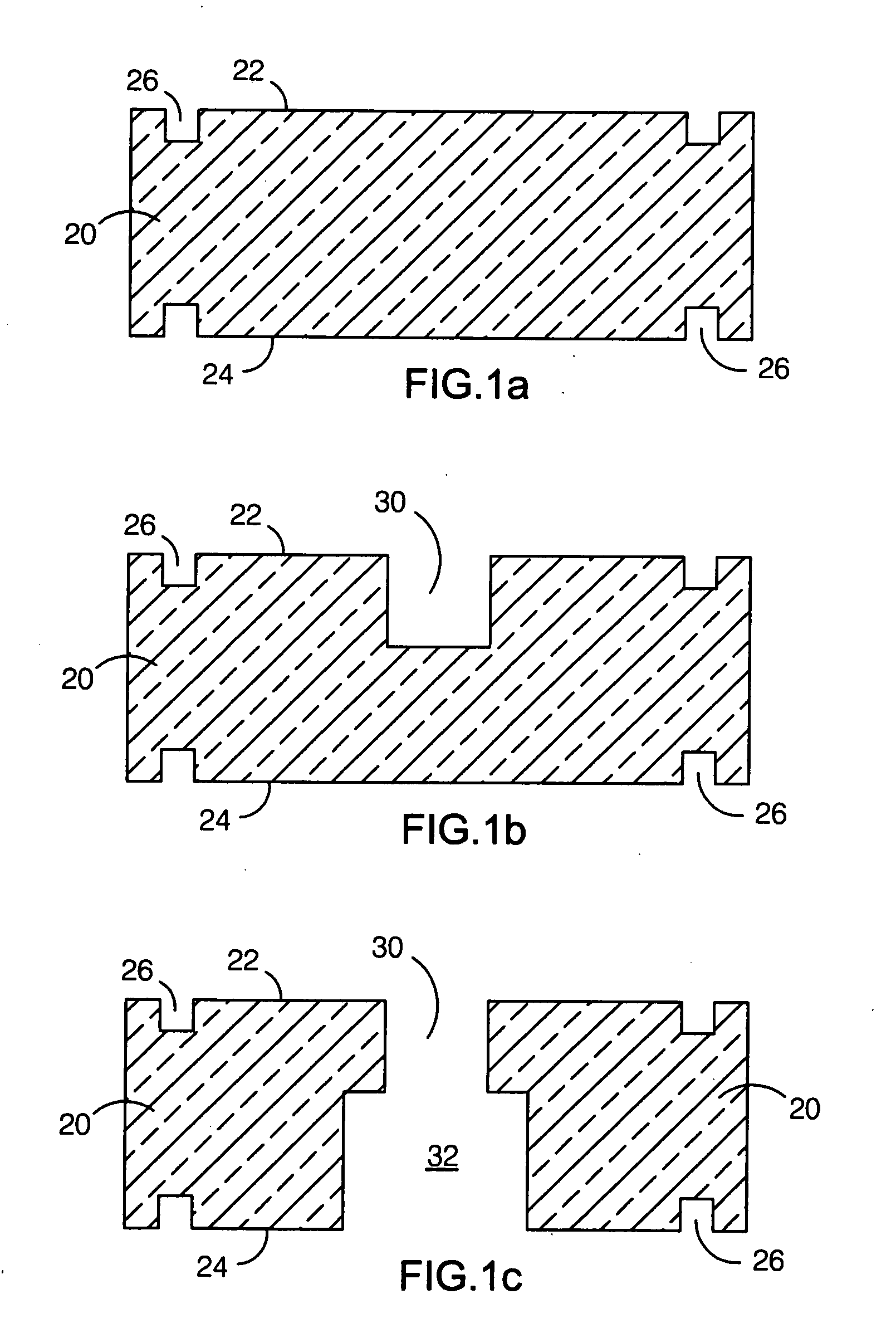
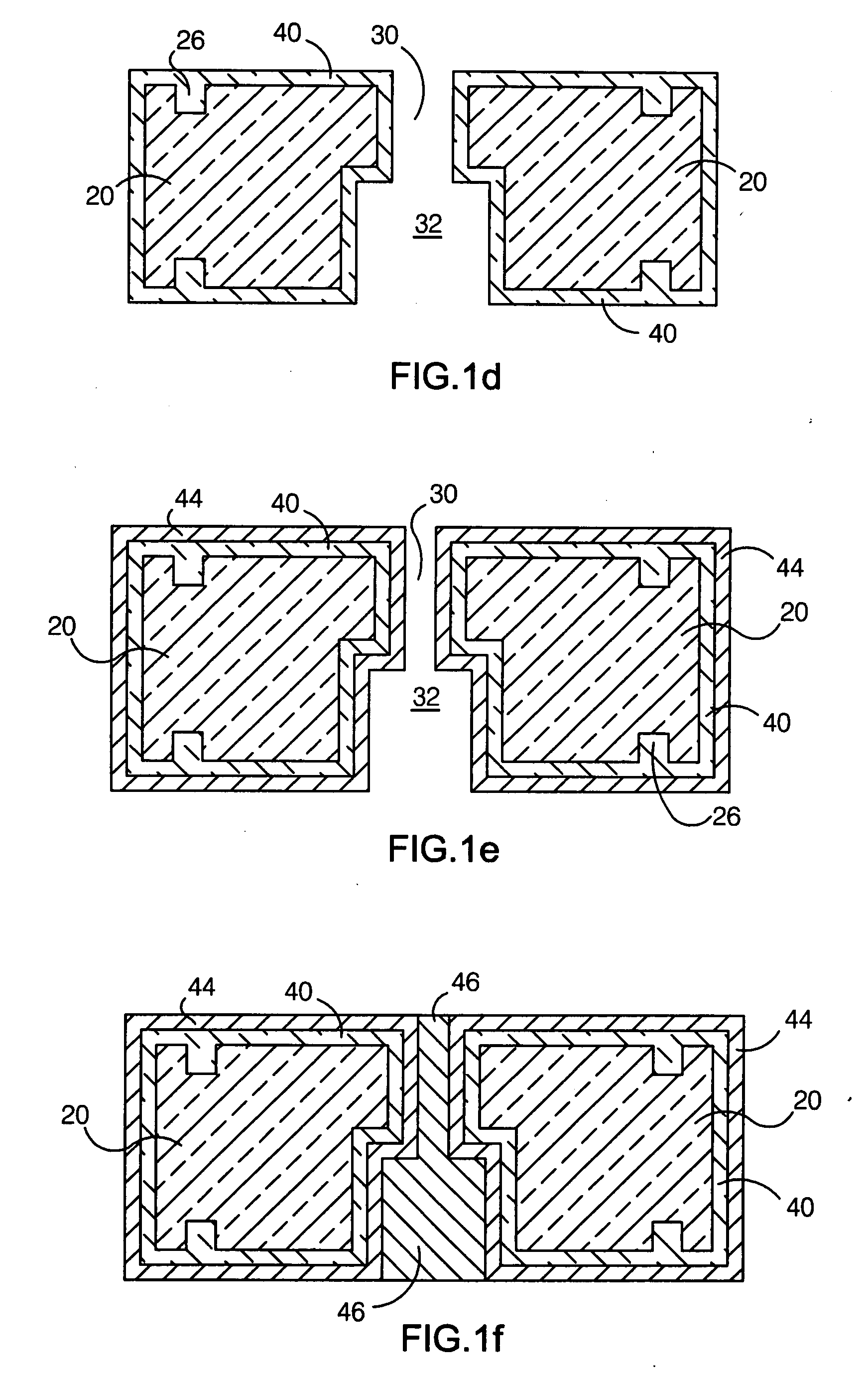
[0016]The present method is directed to a process for fabricating high aspect ratio through-substrate vias. The basic process steps are illustrated in the series of sectional views shown in FIGS. 1a-1g. In FIG. 1a, a substrate 20 has a first surface 22 and a second surface 24. Circuitry (not shown) may be disposed on first surface 22, on second surface 24, and / or between surfaces 22 and 24. The substrate may be made from any of a number of semiconductor materials, including but not limited to, silicon, gallium arsenide or indium phosphate. Alignment marks 26 may be etched on the first and second surfaces, to facilitate alignment of the substrate during subsequent process steps.

[0017]In FIG. 1b, a first cavity 30 is etched into first surface 22. The first cavity has a first diameter, and extends a first depth into the substrate. The first diameter is typically chosen to minimize the consumed circuit area on surface 22. The first depth is typically chosen to enable the first cavity to...


PUM


Abstract

An through-substrate via fabrication method requires forming a through-substrate via hole in a semiconductor substrate, depositing an electrically insulating, continuous and substantially conformal isolation material onto the substrate and interior walls of the via using ALD, and depositing a conductive material into the via and over the isolation material using ALD such that it is electrically continuous across the length of the via hole. The isolation material may be prepared by activating it with a seed layer deposited by ALD. The via hole is preferably formed by dry etching first and second cavities having respective diameters into the substrate's top and bottom surfaces, respectively, to form a single continuous aperture through the substrate. The present method may be practiced at temperatures of less than 200° C. The basic fabrication method may be extended to provide vias with multiple conductive layers, such as coaxial and triaxial vias.

Description

FIELD OF THE INVENTION[0001]This invention is directed to a method for fabricating high aspect ratio through-substrate vias.BACKGROUND[0002]The fabrication of integrated circuit (IC) chips has become a sophisticated process that can allow complex circuitry to be densely packaged onto a single substrate or wafer. Originally, most chips were fabricated in a simple planar design. However, planar chip designs limit the amount of circuitry that can be placed on a single substrate.[0003]To overcome some of the limitations resulting from the planar design, designers began stacking chips to form three-dimensional designs. Vias extending through the substrate—i.e., “through-substrate vias”—create three-dimensional interconnects which facilitate connection to the circuitry throughout the chip, thereby allowing the implementation of more advanced circuits and enabling a higher density of complex circuitry to be placed within a given die area. Furthermore, a three-dimensional design with throug...

Claims


Application Information

Patent Timeline
IPC IPC(8): H01L23/538H01L21/768
CPCH01L21/76898H01L23/481H01L2924/0002H01L2924/00012H01L2924/00
Inventor DENATALE, JEFFREY F.STUPAR, PHILIP A.PAPAVASILIOU, ALEXANDROS P.
Owner TELEDYNE SCI & IMAGING
Why Eureka
Try Eureka