Production method of semiconductor device and bonding film

a production method and semiconductor technology, applied in the direction of individual semiconductor device testing, semiconductor/solid-state device testing/measurement, instruments, etc., can solve the problems of increasing the risk of solder breakage, increasing the reflow temperature, and taking a long time to cope with the narrowing pitch and narrowing, etc., to achieve a pollution-free singulated semiconductor chip

Active Publication Date: 2010-01-07
RESONAC CORP
View PDF4 Cites 36 Cited by
  • Summary
  • Abstract
  • Description
  • Claims
  • Application Information

AI Technical Summary

Benefits of technology

[0045]According to the present invention, the cutting position is recognized by recognizing a circuit pattern in the circuit surface from the surface opposite to the circuit surface of a semiconductor wafer, and therefore, a pollution-free singulated semiconductor chip can be obtained. Moreove

Problems solved by technology

It takes a long time not only to cope with the narrowing pitch and the narrowing gap but to fill the high viscous underfill material using the capillary flow method.
Furthermore, adoption of lead-free solders has increased the reflow temperature.
For this reason, upon cooling after reflow, a stress during contraction due to a difference in the thermal expansion coefficients between the substrate and the semiconductor chip increases the risk that the solder breaks.
However, since the discharge amount of the liquid resin will vary in accordance with the viscosity change of the liquid resin ev

Method used


Image

  • Production method of semiconductor device and bonding film
  • Production method of semiconductor device and bonding film
  • Production method of semiconductor device and bonding film

Examples


first embodiment

[0058]FIG. 1 to FIG. 8 are process charts schematically showing a method of manufacturing semiconductor devices according to a first embodiment.

[0059]Layered Product Preparation Step

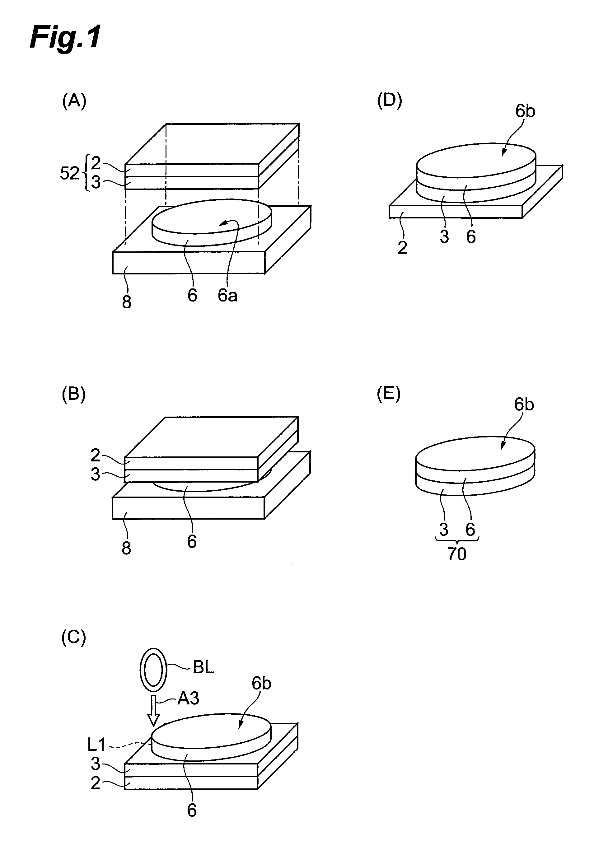
[0060]First, as shown in FIG. 1(A) and FIG. 2(A), for example, a semiconductor wafer 6 such as a silicon wafer is placed on a chuck 8. An electrode pad 7 and an alignment mark 5 are formed in a circuit surface 6a of the semiconductor wafer 6. An insulating film 20 is filled between the electrode pad 7 and the alignment mark 5. The surfaces of the electrode pad 7, the alignment mark 5, and the insulating film 20 are planarized. A projection electrode 4 (terminal) projecting from the surface of the insulating film 20 is provided on the electrode pad 7. The electrode pad 7, the alignment mark 5, and the projection electrode 4 form a circuit pattern P. A rear surface 6b (surface opposite to the circuit surface) of the semiconductor wafer 6 is in contact with the chuck 8.

[0061]On the other hand, an adhesive s...

second embodiment

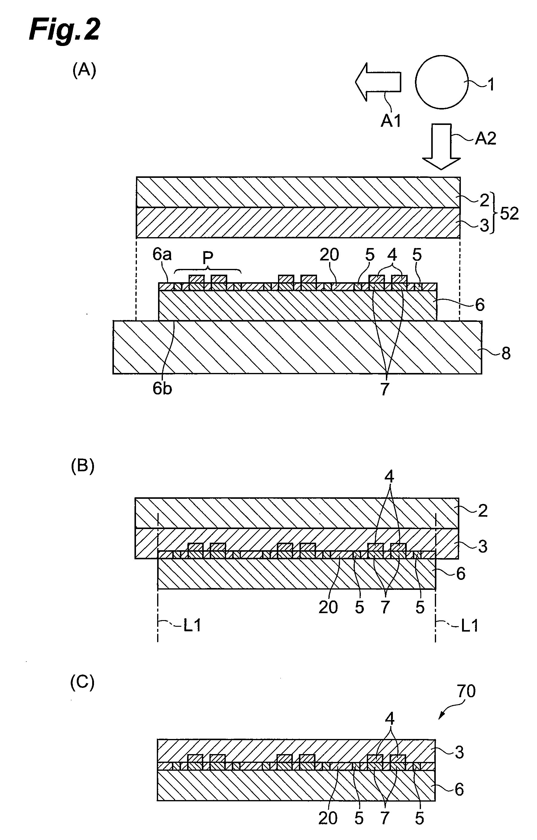
[0104]FIG. 9 is a process chart schematically showing a step in a method of manufacturing semiconductor devices according to a second embodiment. In this embodiment, the adhesive layer 3 of the adhesive sheet 52, which is processed in advance so that the size of the adhesive layer 3 may become substantially the same as the size of the semiconductor wafer 6, is laminated onto the circuit surface 6a. Thereafter, by peeling / removing the separator 2 from the adhesive layer 3, the layered product 70 comprising the semiconductor wafer 6 and the adhesive layer 3 is formed as shown in FIG. 2(C). Thereafter, as in the first embodiment, the semiconductor device 50 shown in FIG. 8(B) can be manufactured. In this embodiment, the same operational effect as that of the first embodiment is obtained. Furthermore, in the case of this embodiment, the cutting step after laminating the adhesive layer 3 onto the semiconductor wafer 6 is not required, thereby increasing the operating efficiency.

[0105]In ...

third embodiment

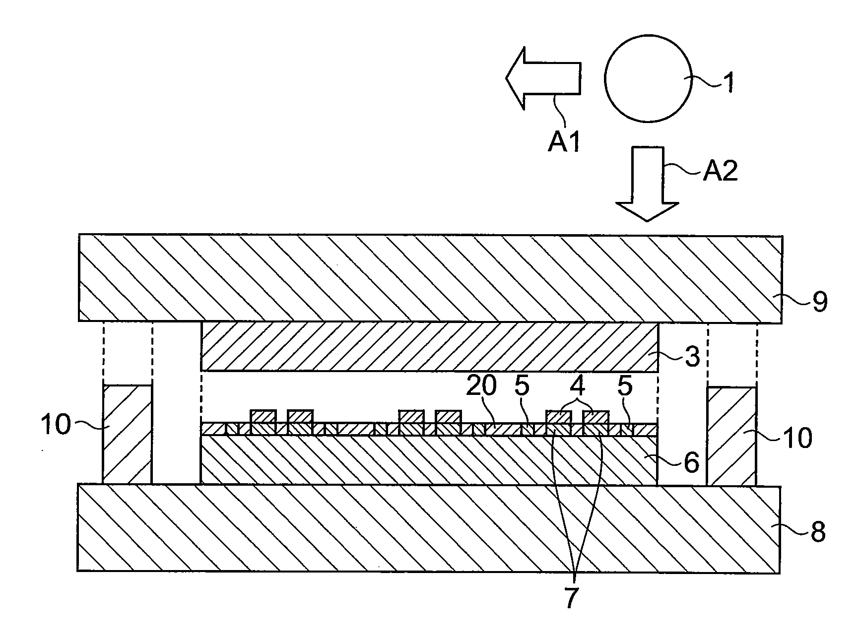
[0106]FIG. 10 is a process chart schematically showing a step in a method of manufacturing semiconductor devices according to a third embodiment. In this embodiment, the adhesive layer 3 is formed on the dicing tape 9. The size of the adhesive layer 3 is processed in advance so as to be substantially the same as the size of the semiconductor wafer 6. On the other hand, the semiconductor wafer 6 and the dicing frame 10 are placed on the chuck 8. Thereafter, the semiconductor wafer 6 is arranged so that the circuit surface 6a thereof may face the adhesive layer 3 side, and then the dicing tape 9, in which the adhesive layer 3 is formed, is laminated onto the circuit surface 6a of the semiconductor wafer 6 using the roller 1. Thus, the structure shown in FIG. 4(B) is obtained. Thereafter, as in the first embodiment, the semiconductor device 50 shown in FIG. 8(B) can be manufactured. In this embodiment, the same operational effect as that of the first embodiment is obtained. Moreover, t...


PUM

PropertyMeasurementUnit
Thicknessaaaaaaaaaa

Abstract

To provide a method of manufacturing semiconductor devices, the method being capable of efficiently obtaining a singulated semiconductor chip upon which an adhesive is adhered and also capable of excellently bonding a semiconductor chip to a wiring substrate, and provide an adhesive film. A layered product 60 in which a dicing tape 9, an adhesive layer 3, and a semiconductor wafer 6 are stacked in this order so that a circuit surface 6a of the semiconductor wafer 6 may face the dicing tape 9 side. A cutting position is recognized by recognizing a circuit pattern P in the circuit surface 6a from a rear surface 6b of the semiconductor wafer 6. At least the semiconductor wafer 6 and the adhesive layer 3 are cut in the thickness direction of the layered product 60. The dicing tape 9 is cured to peel off the dicing tape 9 and the adhesive layer 3. A projection electrode 4 of a semiconductor chip 26 is aligned with a wiring 12 of a wiring substrate 40. The wiring substrate 40 and the semiconductor chip 26 are bonded via an adhesive layer 23 so that the wiring 12 and the projection electrode 4 may be electrically connected to each other.

Description

TECHNICAL FIELD[0001]The present invention relates to a method of manufacturing semiconductor devices, and to adhesive films.BACKGROUND ART[0002]As the method of bonding a semiconductor chip to a substrate, a flip chip bonding method is known. In this bonding method, a semiconductor chip is arranged with the circuit surface thereof facing the substrate side. The electrical connection is made by bonding a projection electrode called a bump formed in the circuit surface of the semiconductor chip to a terminal formed in the substrate. The flip chip bonding method is advantageous in miniaturizing and thinning the structure of a surface-mounted component. Furthermore, the flip chip bonding method is perceived to be advantageous in achieving high speed because the bonding distance is short. In particular, in electronic apparatuses, such as a mobile phone or a Personal Digital Assistant, and a memory card, an IC card, and the like, the number of surface-mounted components manufactured usin...

Claims


Application Information

Patent Timeline
IPC IPC(8): H01L21/60H01L21/301H01L21/683C08L63/00
CPCH01L21/67092H01L2224/81191H01L21/78H01L24/27H01L24/75H01L24/81H01L24/83H01L24/90H01L2221/6834H01L2223/54426H01L2223/54473H01L2224/13144H01L2224/274H01L2224/81121H01L2224/81205H01L2224/81801H01L2224/83191H01L2224/838H01L2224/83851H01L2224/83885H01L2924/01004H01L2924/01013H01L2924/01029H01L2924/01033H01L2924/01046H01L2924/01047H01L2924/01049H01L2924/0105H01L2924/01052H01L2924/01058H01L2924/01077H01L2924/01078H01L2924/01079H01L2924/01082H01L24/29H01L2224/2919H01L2924/01005H01L2924/01006H01L2924/01023H01L2924/01041H01L2924/01045H01L2924/014H01L2924/0665H01L21/6835H01L2924/07811H01L2224/73204H01L2224/73104H01L2224/32225H01L2224/16225H01L2924/00H01L2924/3512H01L2224/0554H01L2224/05568H01L2224/05573H01L2224/05624H01L2224/81193H01L2924/00014H01L2924/15788H01L2224/05599H01L2224/0555H01L2224/0556H01L21/48
Inventor NAGAI, AKIRAYASUDA, MASAAKIHATAKEYAMA, KEIICHIENOMOTO, TETSUYA
Owner RESONAC CORP
Why Eureka
Try Eureka