
Defect Inspection Method and Apparatus

a technology of defect type and inspection method, applied in the direction of mechanical roughness/irregularity measurement, semiconductor/solid-state device testing/measurement, instruments, etc., can solve the problems of difficult to obtain high-precision classification/size determination performance by actual application, low accuracy of classification and size measurement for a plurality of defect types containing various shapes and materials, and long time required for inspection.

Inactive Publication Date: 2010-01-07
HITACHI HIGH-TECH CORP
View PDF23 Cites 71 Cited by
  • Summary
  • Abstract
  • Description
  • Claims
  • Application Information

AI Technical Summary

Benefits of technology

[0005]There has been a demand for high precision classification of various defects and high precision size measurement thereof upon a defect inspection used in a process for manufacturing a semiconductor or the like for early detection of process defective or failure factors of a manufacturing apparatus. The classification of concavo-convex defects by an intensity ratio in two directions between scattered lig

Problems solved by technology

Since, however, the scattered distribution / light amount depends on the shape and material of each defect and changes greatly and non-linearly, the accuracy of classification and size measurement for a plurality of defect types containing various shapes and materials was low.
Although a method for comparing scattered light distributions determined by a simulator with detected outputs is known as a technique for realizing high precision classification and size measurement, the related art has involved a problem that since there is a need to perform inspection plural times by switching of filters in order to obtain signals corresponding to a plurality of detection directions, the time necessary for the inspection becomes long.
Further, there occurs a dissociation between each of actually-obtained detected outputs and each calculated value determined by simulation due to the influences of individual differences of an illumination section, a detection section, a signal processing section and the like, deviations / variations for adjustment, and errors caused by the accuracy of a simulation model and the like, it was difficult to obtain high precision classification / size determination performance by actual application of the above.

Method used


Image

  • Defect Inspection Method and Apparatus
  • Defect Inspection Method and Apparatus
  • Defect Inspection Method and Apparatus

Examples


Embodiment Construction

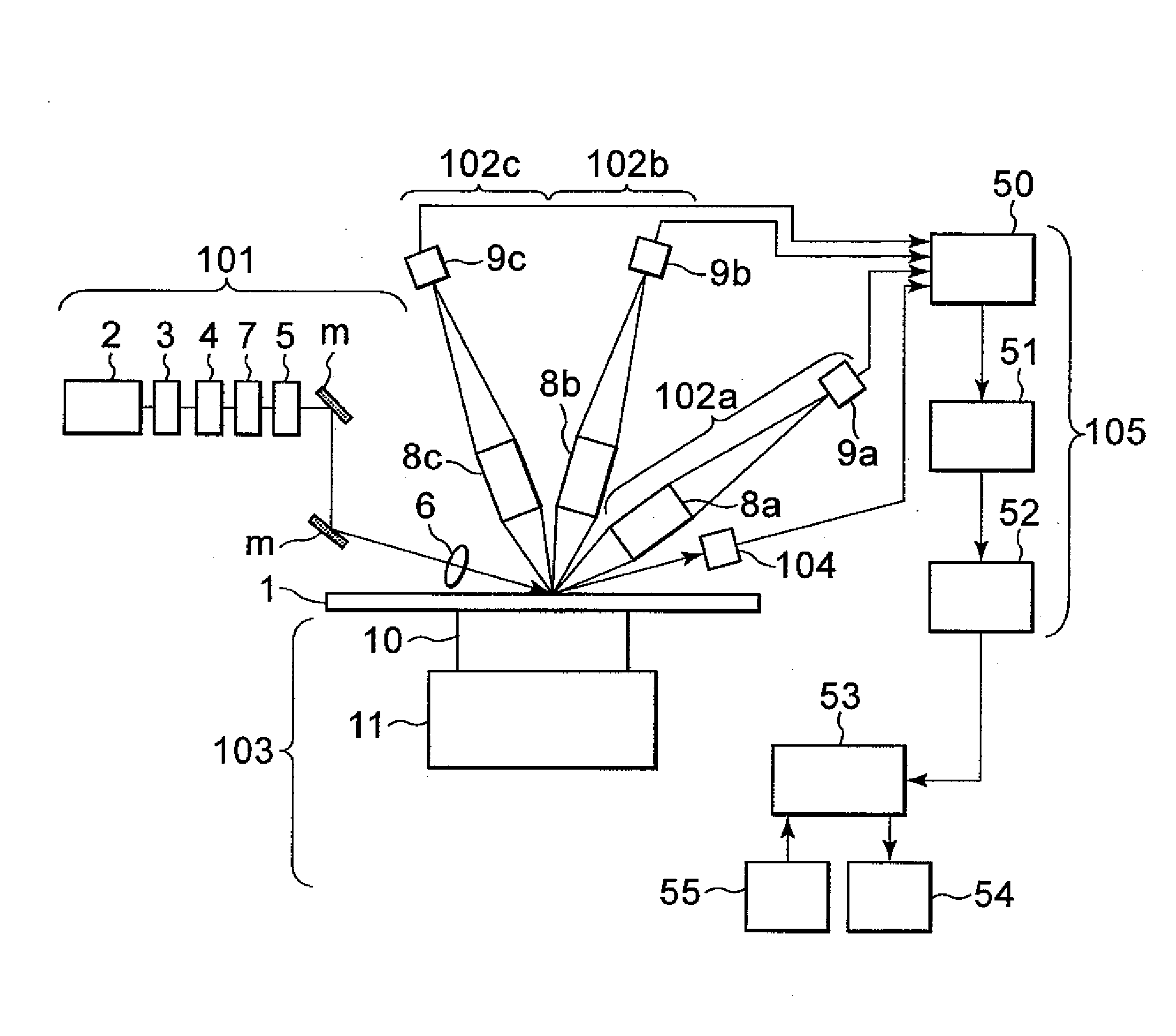
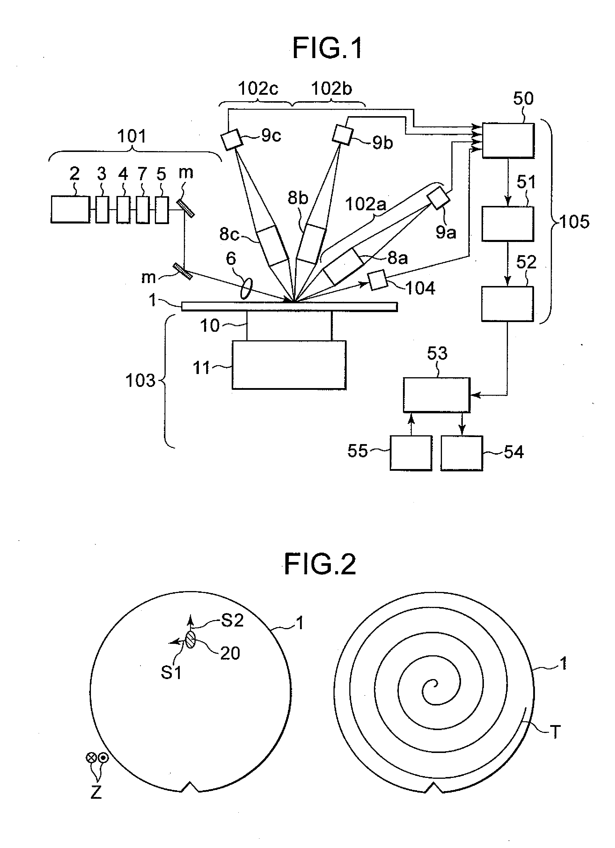
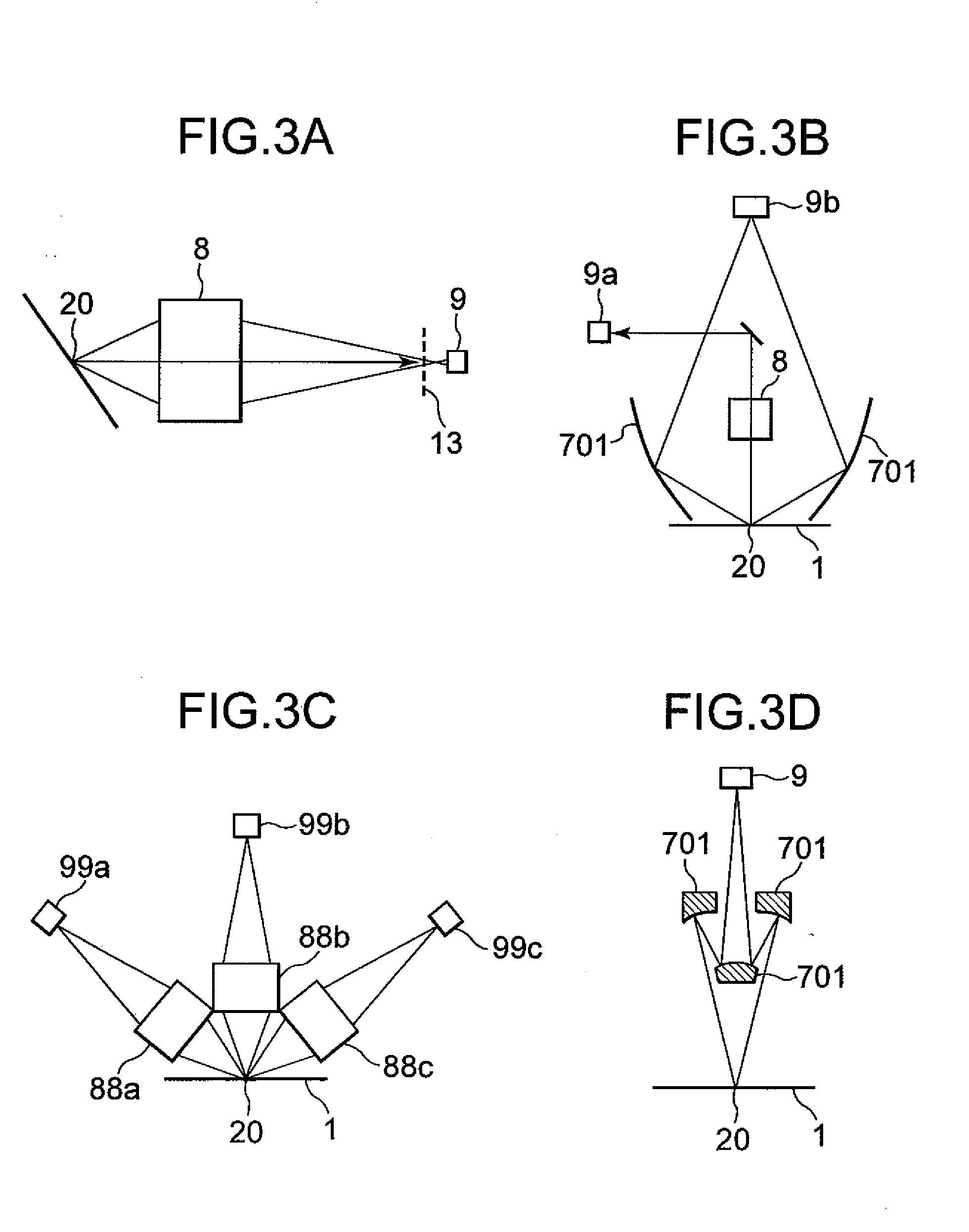
[0062]A configuration of an embodiment of the present invention will be explained using FIG. 1. The present embodiment is configured using suitably an illumination section 101, a detection section 102 (102a, 102b and 102c), a stage 103 capable of placing a sample 1 thereon, a signal processing section 105, an overall control unit 53, a display unit 54 and an input unit 55. The signal processing section 105 has a defect determination unit 50, a feature extraction unit 51 and a defect type / size determination unit 52. A specular reflection detecting unit 104 is provided as needed for the purpose of a large area defect inspection or sample surface measurements and the like.

[0063]The illumination section 101 is configured using suitably a laser light source 2, an attenuator 3, a polarizing device or element 4, a beam expander 7, an illumination distribution control element 5, a reflection mirror m and a condensing lens 6. Laser light emitted from the laser light source 2 is adjusted to a...


PUM


Abstract

In a detection step, light produced on a sample in plural directions are collectively detected using a plurality of detectors. Multidimensional features containing information about scattered light distributions are extracted based on a plurality of detector outputs obtained. The feature is compared with data in a scattered light distribution library thereby to determine the types and sizes of defects. In a feature extraction step, a feature outputted based on the magnitude of each of scattered light detected signals of scatterers already known in refractive index and shape, which are obtained in the detection step, is corrected, thereby realizing high precision determination.

Description

BACKGROUND OF THE INVENTION[0001]The present invention relates to a defect inspection method and apparatus for inspecting micro defects existing in the surface of a sample to determine the type and size of each defect and outputting the same.[0002]It has been practised to inspect defects existing in the surfaces of a semiconductor substrate and a thin-film substrate or the like on a line for manufacturing the semiconductor substrate and the thin-film substrate or the like with a view toward maintaining / improving the yield of each product. JP-A-9-304289 (patent document 1), JP-A-2006-201179 (patent document 2), etc. have been known as related arts. In order to detect micro defects, a laser beam focused to a few tens μm is applied onto the surface of a sample to collect and detect scattered light from the defects, thereby inspecting the defects each having a size ranging from a few tens nm to a few μm or more. There has thus been described a technique for detecting a component of each...

Claims


Application Information

Patent Timeline
IPC IPC(8): G01N21/88G06F19/00G01N21/956H01L21/66
CPCG01N21/4738G01N2021/887G01N2021/4711G01N21/9501
Inventor URANO, YUTAHONDA, TOSHIFUMIHAMAMATSU, AKIRAMAEDA, SHUNJI
Owner HITACHI HIGH-TECH CORP
Features
  • Generate Ideas
  • Intellectual Property
  • Life Sciences
  • Materials
  • Tech Scout
  • Unparalleled Data Quality
  • Higher Quality Content
  • 60% Fewer Hallucinations
Learn More