Photoelectric conversion apparatus, imaging system, and photoelectric conversion apparatus manufacturing method
- Summary
- Abstract
- Description
- Claims
- Application Information
AI Technical Summary
Benefits of technology
Problems solved by technology
Method used
Image

Examples
Embodiment Construction
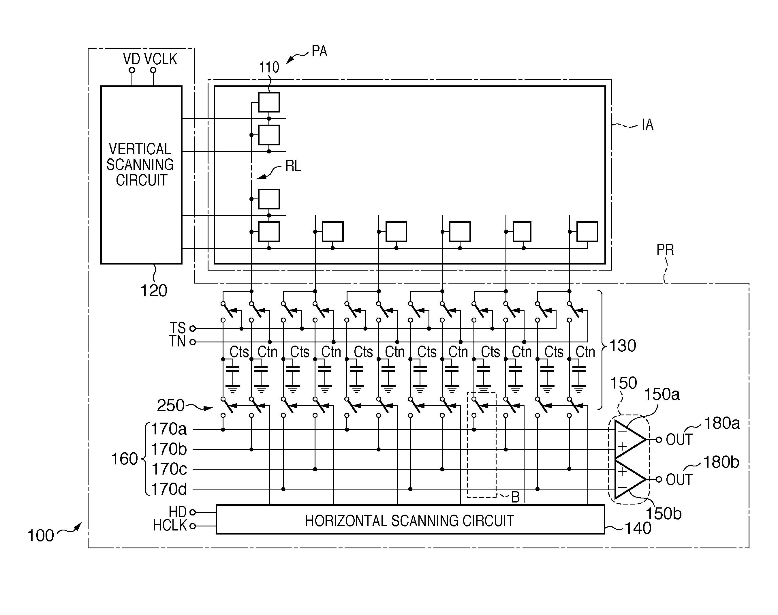
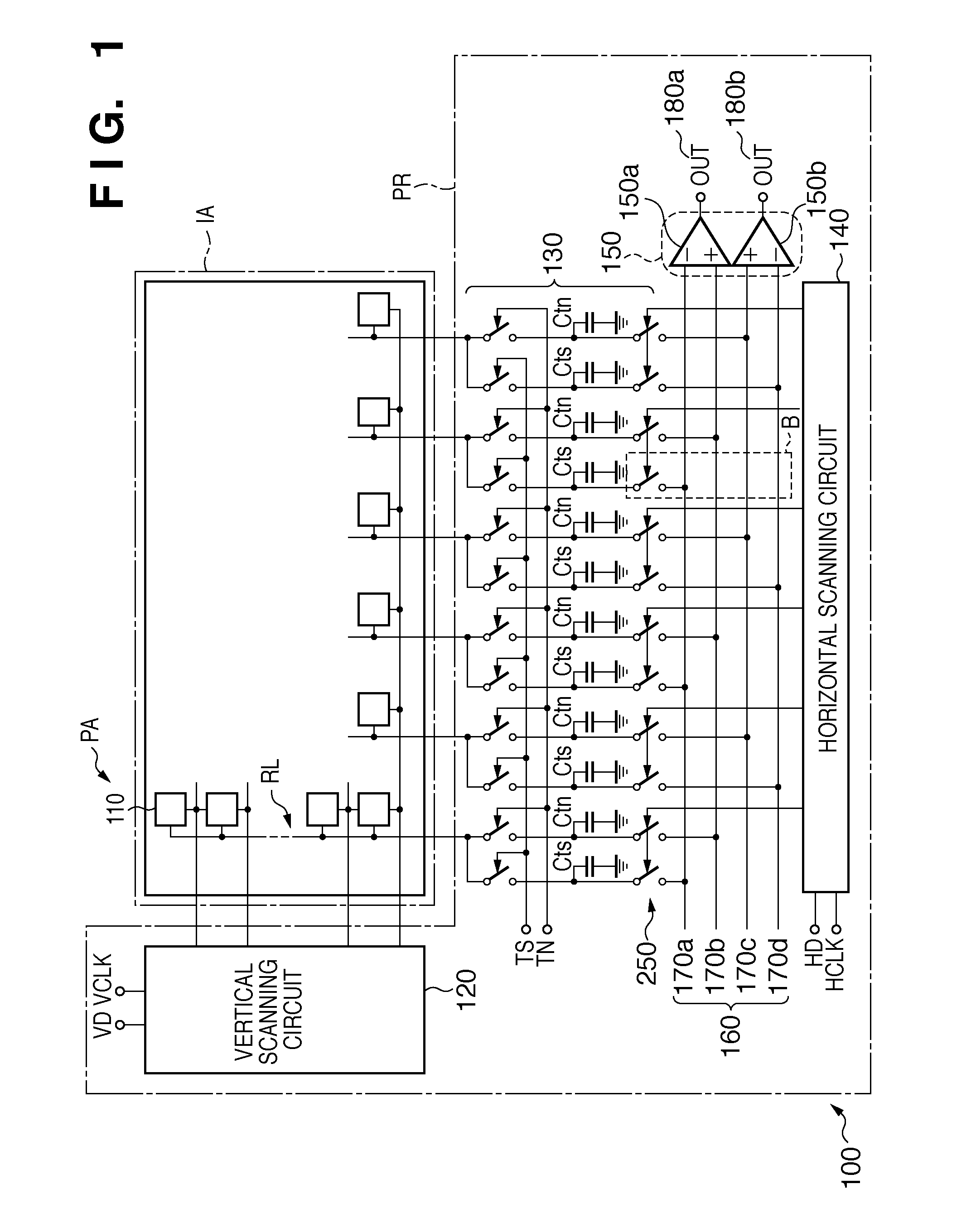
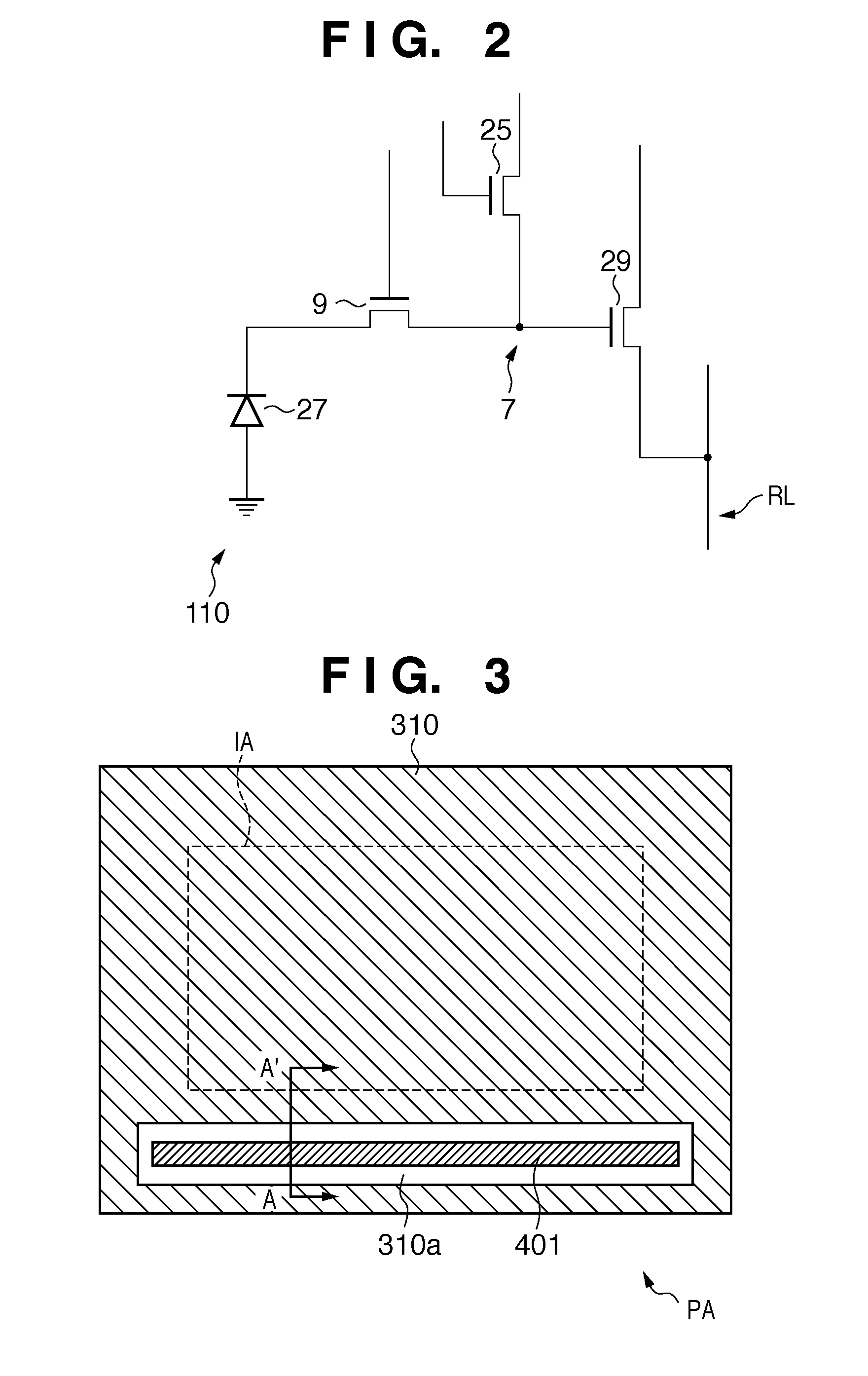
[0026]The arrangement of a photoelectric conversion apparatus 100 according to the first embodiment of the present invention will be described with reference to FIGS. 1 to 3. FIG. 1 is a diagram of the arrangement of the photoelectric conversion apparatus 100 according to the first embodiment of the present invention. FIG. 2 is a circuit diagram showing the structure of a pixel in the photoelectric conversion apparatus 100. FIG. 3 is a plan view showing the structure of a color filter layer in the photoelectric conversion apparatus 100.
[0027]The photoelectric conversion apparatus 100 includes a pixel array region IA and peripheral region PR. The pixel array region IA is, for example, a region where an object image is formed and sensed. The peripheral region PR is positioned at the periphery of the pixel array region IA.
[0028]A pixel array PA is arranged in the pixel array region IA. The peripheral region PR includes a vertical scanning circuit 120, readout circuit (readout unit) 130...
PUM
 Abstract
Description
Claims
Application Information
 - Generate Ideas
- Intellectual Property
- Life Sciences
- Materials
- Tech Scout
- Unparalleled Data Quality
- Higher Quality Content
- 60% Fewer Hallucinations
Browse by: Latest US Patents, China's latest patents, Technical Efficacy Thesaurus, Application Domain, Technology Topic, Popular Technical Reports.
© 2025 PatSnap. All rights reserved.Legal|Privacy policy|Modern Slavery Act Transparency Statement|Sitemap|About US| Contact US: help@patsnap.com