Light emitting device and method for producing the light emitting device

a light emitting device and light technology, applied in the field can solve the problems of device increase, low heat resistance of fluorescent materials in sealing resins, and low emission efficiency of light emitting devices, and achieve the effects of increasing luminous flux, high heat resistance properties, and not reducing emission efficiency

Inactive Publication Date: 2010-01-14
USHIO DENKI KK
View PDF5 Cites 16 Cited by
  • Summary
  • Abstract
  • Description
  • Claims
  • Application Information

AI Technical Summary

Benefits of technology

[0021]According to the present invention, since an SiC fluorescent screen has a high heat resistance property, the emission efficiency does not decline when in use, unlike a conventional device. Moreover, since the heat resistance of the device increases as a whole, it becomes possible to increase luminous flux by delivering a high electric current to the LED elements. Furthermore, white light of good color rendition can be generated because an SiC fluorescent screen can emit radiation having a large full width at half maximum compared with that of LED elements and the like when excited by radiation emitted from the first LED elements.
[0022]Furthermore, heat generated from each LED element can smoothly be transmitted to a substrate because the substrate is bound to each element by an AuSn type alloy layer having columnar crystals.

Problems solved by technology

However, in the light emitting device described in Japanese Patent Application Publication No. 2003-535478 and corresponding U.S. Pat. No. 6,504,179, the heat resistance of the fluorescent material is low in the sealing resin, and the emission efficiency of the light emitting device declines when the temperature of the device increases when in use.
Moreover, since the heat quantity of an LED element is restricted, it is difficult to increase luminous flux by flowing a high electric current to the LED element.
However, the full width at half maximum of each LED element is extremely small compared with that of a fluorescent material, the color rendition of white light generated declines.

Method used


Image

  • Light emitting device and method for producing the light emitting device
  • Light emitting device and method for producing the light emitting device
  • Light emitting device and method for producing the light emitting device

Examples


Embodiment Construction

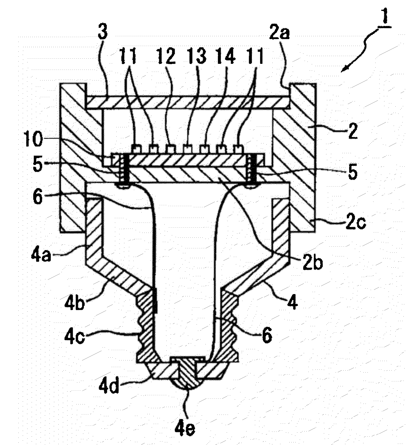
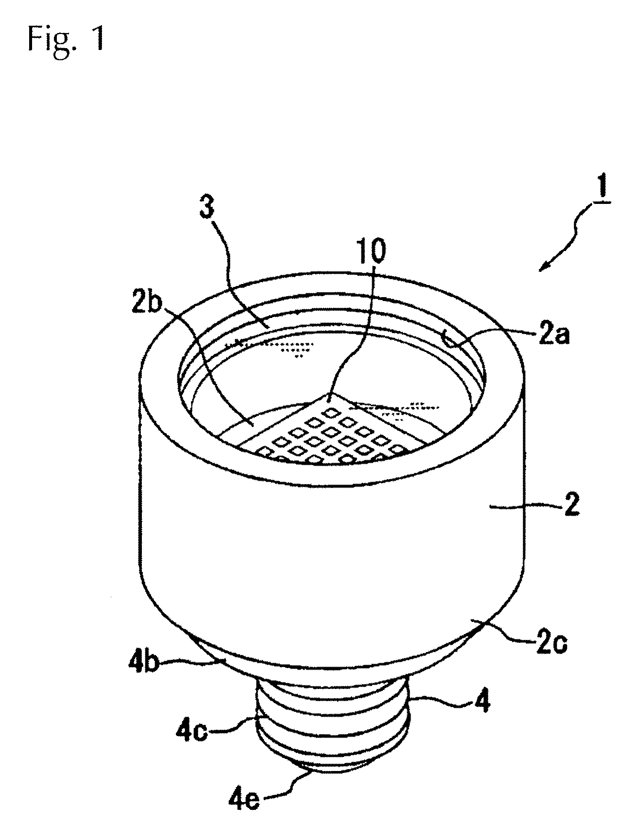
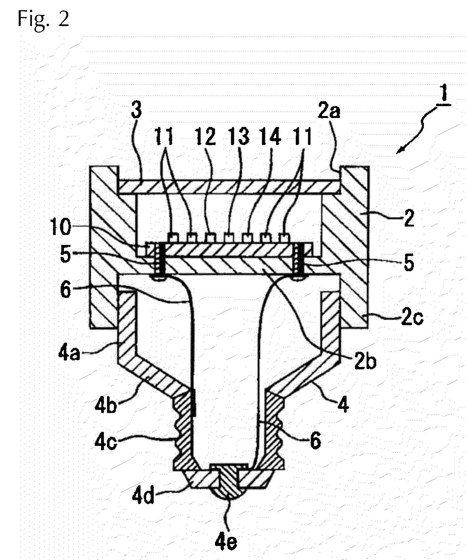
[0033]As shown in FIG. 1, a light emitting device 1 has a cylindrical body 2 with an opening 2a formed on one end, an SiC fluorescent screen for closing the opening 2a, and an electric terminal part 4 formed on the other end of the body 2. In the present embodiment, a description is given such that the one end of the body 2 is in the upward direction and the other end in the downward direction. In the body 2 are contained multiple types of LED elements to which electric power is supplied from the electric terminal part 4. A SiC fluorescent screen 3 is excited by UV radiation emitted from the LED elements to emit light. Blue light, green light and red light emitted from the LED elements pass through the SiC fluorescent screen 3 without going through any conversion in their wavelengths.

[0034]FIG. 2 is a schematic vertical sectional view of the light emitting device.

[0035]The body 2 shown in FIG. 2 is made of inorganic material. Its lower end is closed off, and the closed part constitu...


PUM


Abstract

A light emitting device that has a radiant efficiency that does not decline in use, enables luminous flux to be increased by a high electric current, and produces white light with good color rendering and a method for producing a light emitting device capable of smoothly transmitting heat generated by LED elements to a carrier substrate. The radiation emitting device has first LED elements for emitting UV radiation, second LED elements for emitting visible light, a substrate made of an inorganic material and which carries the first LED elements and the second LED elements, a body made of inorganic material containing the first LED elements, the second LED elements and the substrate, and an SiC fluorescent screen that is doped with at least one of B and Al as well as N and emits visible light when excited by radiation emitted from the first LED elements.

Description

BACKGROUND OF THE INVENTION[0001]1. Field of Invention[0002]This invention relates to a light emitting device that is provided with LED elements and emits white light.[0003]2. Description of Related Art[0004]A light emitting device has conventionally been known that emits white light by combining an LED element and fluorescent material (see, e.g., Japanese Patent Application Publication No. 2003-535478 and corresponding U.S. Pat. No. 6,504,179). The light emitting device described in this document is provided with an LED element that emits radiation of 300-470 nm and generates white light as a result of this light being converted into light having a longer wavelength fully or partially by the fluorescent material excited by this radiation. The fluorescent material is dispersed in sealing resin that seals the LED element.[0005]A light emitting device has also been known that can generate white light by combining a red LED element, a green LED element and a blue LED element (See, e.g....

Claims


Application Information

Patent Timeline
Patent Type & Authority Applications(United States)
IPC IPC(8): H01L33/00H01L21/50
CPCF21K9/13F21S48/1159F21V5/005F21V19/0055F21Y2101/02F21Y2113/005H01L33/62H01L2224/48091H01L2224/48137H01L2224/48227H01L2224/73265H01L2224/92247F21K9/56F21S48/1145H01L2924/00012F21V3/049F21Y2105/12F21Y2105/10F21K9/23F21K9/64F21Y2115/10F21Y2113/13F21S41/14F21S41/147F21V3/08F21V5/10F21S41/153F21S41/176
Inventor IMAI, YUJIKAMIYAMA, SATOSHI
Owner USHIO DENKI KK
Why Eureka
Try Eureka