Surface inspecting method and device

a surface inspection and inspection method technology, applied in the direction of optical radiation measurement, semiconductor/solid-state device testing/measurement, instruments, etc., can solve the problem that the influence of a wafer base material cannot be quantitatively measured and the calibration of soi wafers cannot be performed by the surface inspection of the conventional dual-wavelength method. achieve the effect of accurately measuring the inside of the body

Inactive Publication Date: 2010-01-14
KK TOPCON
View PDF6 Cites 25 Cited by
  • Summary
  • Abstract
  • Description
  • Claims
  • Application Information

AI Technical Summary

Benefits of technology

[0008]It is an object of the present invention to provide a surface inspection method and an apparatus, which are capable of ac

Problems solved by technology

SOI calibration cannot be performed by the surface inspection of a conventional dual-wavelength method.
In addition, it has been impossible to quantitatively measure the information of interior interface of an SOI wafer.
Although foreign particle measurement on the surface of a thin film SOI wafer of the next generation can be performed by using a short wavelength (DUV), influe

Method used


Image

  • Surface inspecting method and device
  • Surface inspecting method and device
  • Surface inspecting method and device

Examples


Embodiment Construction

[0088]The principle of a measurement method in a preferable example of the present invention will be described.

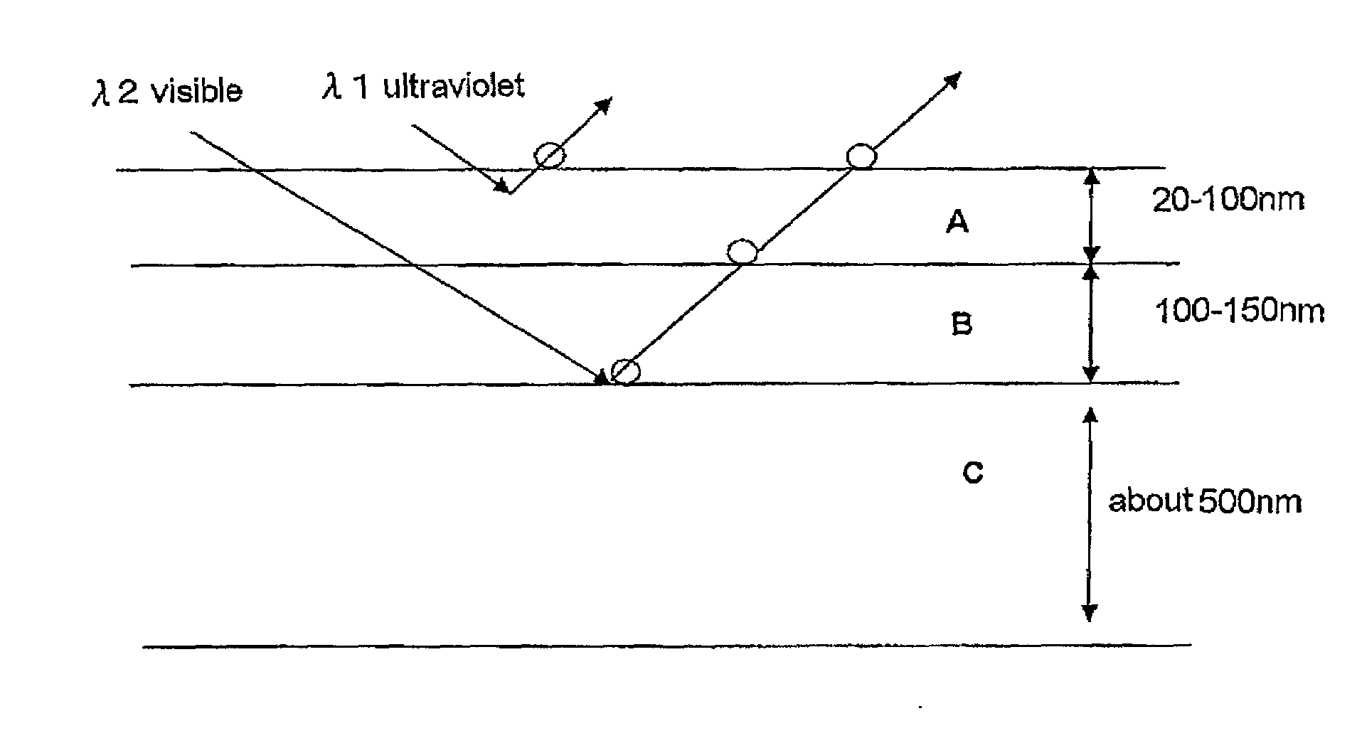
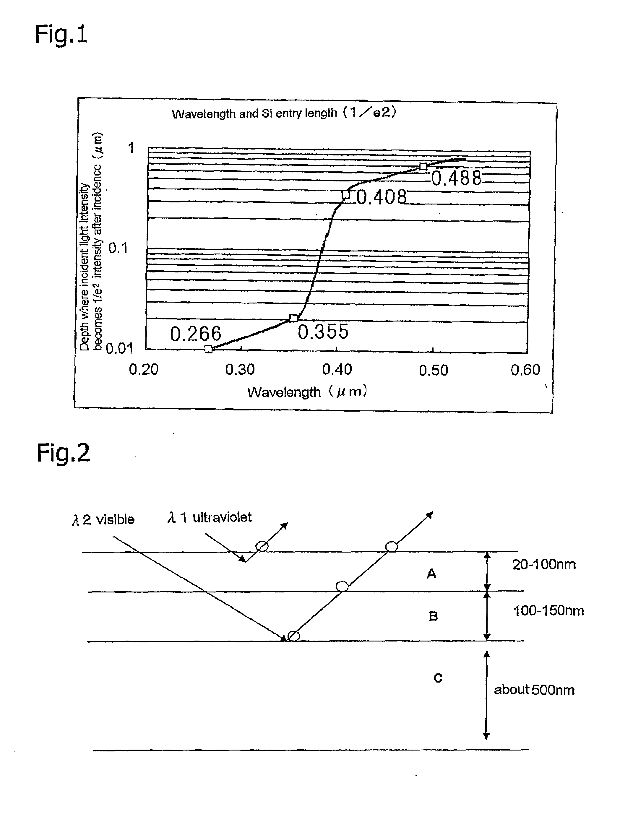
[0089]Relationship between depth and wavelength where incident light intensity becomes 1 / e2 (approximately 13%) in Si by each wavelength is as shown in the graph of FIG. 1.

[0090]As it is clear from FIG. 1, in a region between wavelength of the ultraviolet region (particularly, deep ultraviolet region) and wavelength of the visible region, transmitting distance in Si drastically changes so as to be different by 10 times or more. Therefore, in the case of detecting by irradiating the light having a wavelength in the ultraviolet region, it only detects foreign particles or COP on approximate surface, whereas it is irradiated deep inside the wafer when light having a wavelength in the visible region is used. For this reason, detection of film constitution (multiple structure) inside the wafer, which is COP (COP having the largest number and most characteristic) on the boundary ...


PUM


Abstract

A light source section outputs optical flux having two types of wavelength, which are a short wavelength and a long wavelength, while the intensity is made variable. The optical flux is made incident to a detected surface of a body to be detected at a predetermined incident angle simultaneously or alternatively. Based on a type of optical flux outputted from the light source section and an output from a first light intensity detecting section, at least the intensity of the optical flux having a long wavelength outputted from the light source section is adjusted. The output from the first light intensity detecting section in irradiating the optical flux having a short wavelength is compared with the output from the first light intensity detecting section in irradiating the optical flux having a long wavelength. A signal that appears only in the output from the first light intensity detecting section in irradiating the optical flux having a long wavelength is identified as a detected signal from an internal subject. The intensity of optical flux having a long wavelength is adjusted. A disappearance level near a point where the detected signal from the internal subject disappears is calculated. The first intensity of optical flux having a long wavelength is set to level higher than the disappearance level. Based on the output from the first light intensity detecting section obtained by the optical flux having a long wavelength of the first intensity, a subject inside the body to be detected is measured.

Description

BACKGROUND OF THE INVENTION[0001]1. Field of the Invention[0002]The present invention relates to a method and an apparatus for inspecting the surface of a semiconductor wafer or other body to be detected.[0003]2. Related Art[0004]A method and an apparatus in which defects inside a wafer is inspected by using dual-wavelength laser beam are publicly known. See Japanese Patent Unexamined Publications No. 11-354598, No. 11-237226, and Paper “Measuring technology of the size and the depth of surface defects on the entire wafer surface caused by two-wavelength beam scattering (OSDA: Optical Shallow Defect Analyzer)” written by Takeda Kazuo in Journal of Surface Science and Nanotechnology vol. 22, No. 5, pp. 323-331, 2001.[0005]For example, internal measurement and surface measurement of a wafer are made possible by a wavelength difference between two wavelengths (difference between a short wavelength and a long wavelength).[0006]SOI calibration cannot be performed by the surface inspectio...

Claims


Application Information

Patent Timeline
IPC IPC(8): G01N21/956H01L21/66G01J3/00G01N21/00
CPCG01N21/47G01N21/55G01N21/8422G01N2201/06113G01N21/9501G01N21/9505G01N21/94G01N21/956G01N21/88G01B11/30H01L22/00
Inventor ISOZAKI, HISASHITAKASE, TAKEHIROKAKINUMA, TAKASHIMAEKAWA, HIROYUKIKODA, FUMIOYAMAZAKI, MICHIHIRO
Owner KK TOPCON
Why Eureka
Try Eureka