Surface mount package with high thermal conductivity

Inactive Publication Date: 2010-01-21
HCC AEGIS
View PDF0 Cites 12 Cited by
  • Summary
  • Abstract
  • Description
  • Claims
  • Application Information

AI Technical Summary

Benefits of technology

[0016]The details of one or more embodiments of the invention are set forth in the accompanying drawings and the description below. Other features, objects and advantages of the invention will be apparent from the description and drawings, and from the claims.
[0017]Disclosed herein is a package for use in encapsulating an electronic device is disclosed. In some embodiments, the package includes the following: a dielectric frame having first and second sides, an aperture, a raised shelf portion defined along an internal perimeter of the dielectric frame and extending outwardly from the second side, the raised shelf portion defining a first thickness of the dielectric frame, and a raised sidewall extending outwardly from the second side along an external perimeter of the dielectric frame, the raised sidewall defining a second thickness of the frame, the second thickness being greater than the first thick

Problems solved by technology

As electronic devices become more complex and available space is reduced, the desirability of a surface mount package increases.
Concurrently, as the device complexity increases, the heat generated by operation increases.
If the heat is not removed, the temperature of the device rises shortening the operational life.
Aluminum nitride and silicon carbide are more expensive than alumina and more difficult to shape.
A disadvantage with this approach is that an insulative alumina layer is disposed between the integrated circuit device and the heat sink.
The removal of heat from the chip is limited by the conduction of heat through the alumina layer.
An infiltrated base has limitations.
Any air gaps will reduce thermal conductivity.
When the concentration of the tungsten is high, above about 65% by volume (80% by weight), the infiltrated composite becomes difficult to shape by forging or other deformation processes.
Machining is required, necessitating piece-by-piece manufacture and the generation of scrap increasing the cost of the composite.
Known packages can have limitations at very low temperatures, e.g., in the cryogenic range, as found for applications in deep space.
When exposed to very low temperatures, surface mount packages soldered to a printed circuit board can crack and lose hermeticity.

Method used


Image

  • Surface mount package with high thermal conductivity
  • Surface mount package with high thermal conductivity
  • Surface mount package with high thermal conductivity

Examples


Embodiment Construction

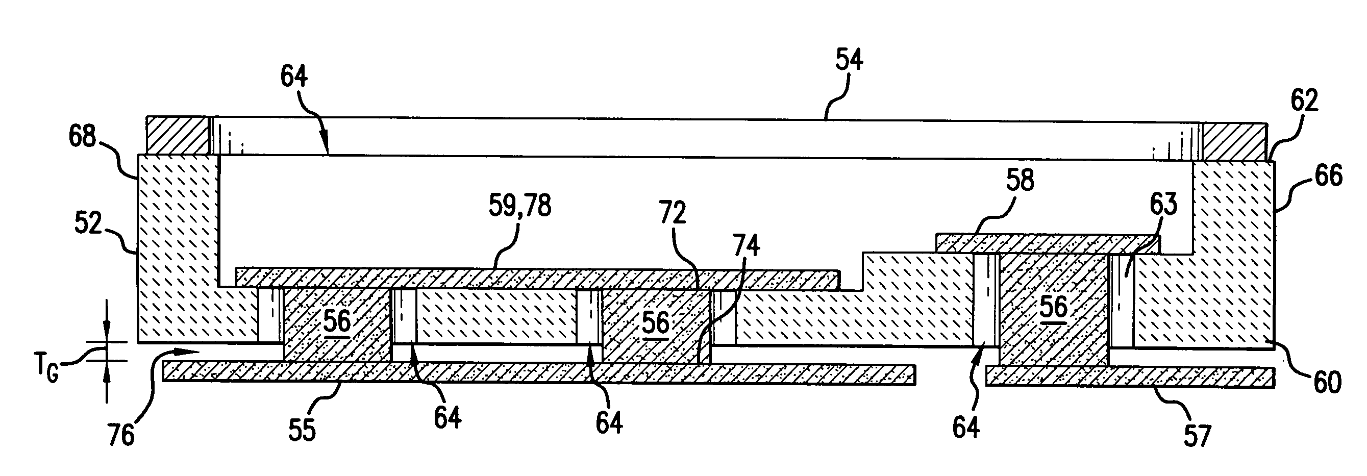
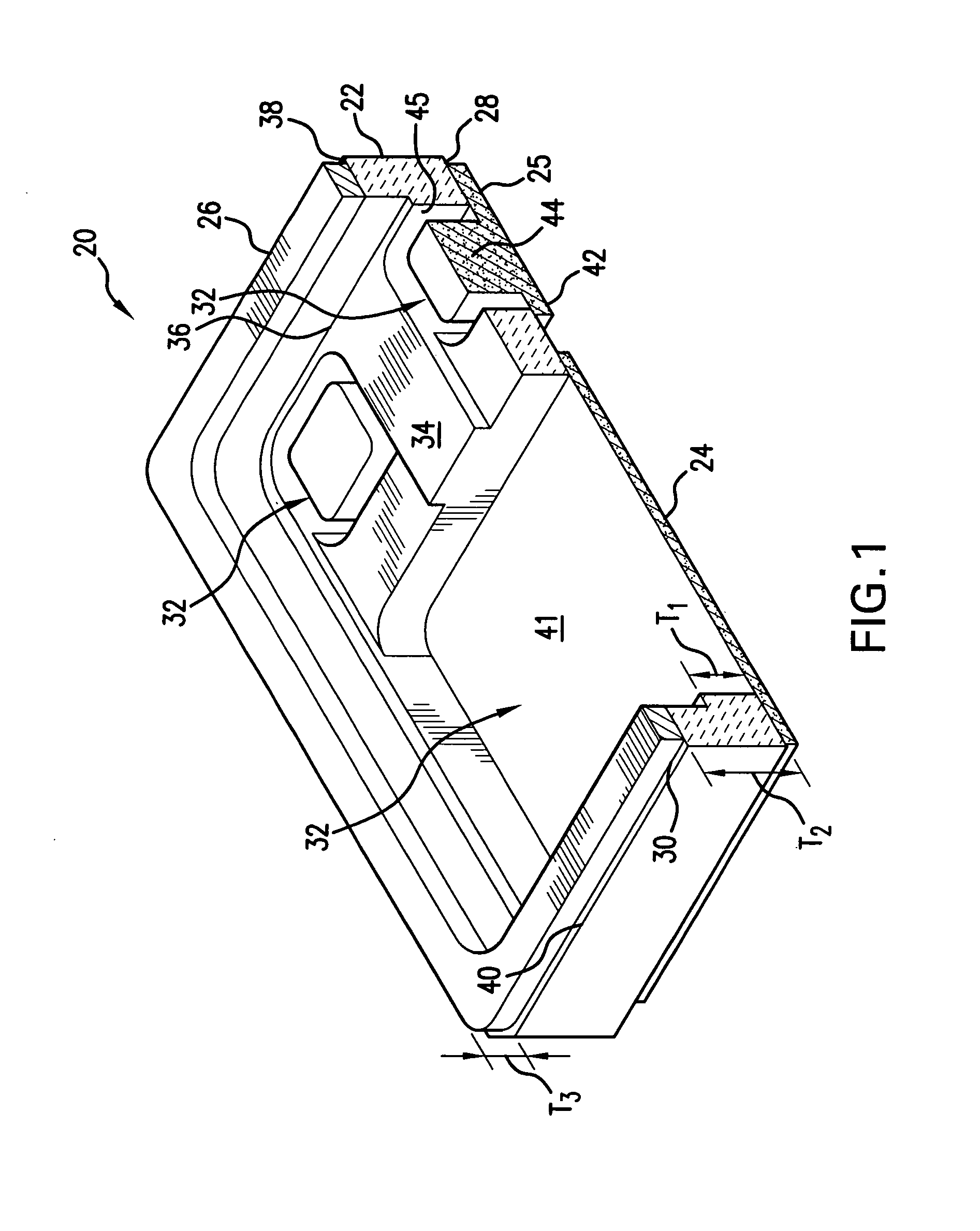
[0027]Generally, the disclosed subject matter relates to a package for housing an electronic circuit. As shown in FIGS. 1 and 2, some embodiments include a package 20 for use in encapsulating an electronic device, such as a semiconductor based integrated circuit or a hybrid circuit having both semiconductor devices and passive devices. Package 20 typically includes a dielectric frame 22, an electrically conductive chip attach pad 24, one or more electrically conductive wire bonding pedestals 25, and a seam weldable, low-profile metallic seal ring 26, all of which are bonded together.

[0028]Dielectric frame 22 includes first and second sides, 28 and 30, respectively, an aperture or apertures 32, and a raised shelf portion 34 defined along an internal perimeter 36 of the dielectric frame and extending outwardly from the second side, and a raised sidewall 38 extending outwardly from the second side along an external perimeter 40 of the dielectric frame. Raised shelf portion 34 defines a...


PUM


Abstract

A package for use in encapsulating an electronic device is disclosed. In some embodiments, the package includes the following: a dielectric frame having first and second sides, an aperture, a raised shelf portion defined along an internal perimeter of the dielectric frame and extending outwardly from the second side, the raised shelf portion defining a first thickness of the dielectric frame, and a raised sidewall extending outwardly from the second side along an external perimeter of the dielectric frame, the raised sidewall defining a second thickness of the frame, the second thickness being greater than the first thickness; a metallic component bonded to the dielectric frame and extending across the aperture; and a seam weldable, low-profile metallic seal ring bonded to the raised sidewall of the dielectric frame. In some embodiments, the package includes the following: a dielectric frame having first and second sides and an aperture, the dielectric frame having an aperture thickness bordering the aperture; a metallic insert positioned within the aperture, the metallic insert having first and second sides, the metallic insert being sized so as to be movable within the aperture and the metallic insert having an insert thickness that is greater than the aperture thickness of the dielectric frame; a first metallic component bonded to the first side of the metallic insert and extending across the aperture; and a second metallic component bonded to the second side of the metallic insert and extending across the aperture.

Description

CROSS REFERENCE TO RELATED APPLICATION(S)[0001]This patent application relates to and claims priority to U.S. Patent Application Ser. No. 61 / 061,887 titled “Surface Mount Device with High Thermal Conductivity” that was filed on Jun. 16, 2008. U.S. Provisional Patent Application Ser. No. 61 / 061,887 is incorporated by reference in its entirety herein.U.S. GOVERNMENT RIGHTS[0002]N.A.BACKGROUND[0003]1. Field of the Invention[0004]The disclosed subject matter relates generally to a package for housing an electronic circuit. More particularly, the disclosed subject matter relates to a surface mount package having a composite metal base supported by a dielectric frame with raised sidewalls and a surface mount package having a dielectric frame and floating metallic components.[0005]2. Description of the Related Art[0006]Increasingly complex microelectronic circuits such as silicon semiconductor integrated circuits and hybrid microelectronic circuits require packages, which both encase the c...

Claims


Application Information

Patent Timeline
IPC IPC(8): H01L23/045
CPCH01L23/055H01L2924/01079H01L2924/09701H01L2924/0002H01L2924/00
Inventor MEDEIROS, III, MANUEL
Owner HCC AEGIS
Why Eureka
Try Eureka