

Power semiconductor device
a technology of power semiconductor and semiconductor device, which is applied in the direction of semiconductor device, semiconductor/solid-state device details, electrical apparatus, etc., can solve the problems of power semiconductor device inability to reduce in size, long manufacturing time, low productivity, etc., and achieve the effect of improving productivity and reducing siz
- Summary
- Abstract
- Description
- Claims
- Application Information
AI Technical Summary
Benefits of technology
Problems solved by technology
Method used
Image

Examples
first embodiment
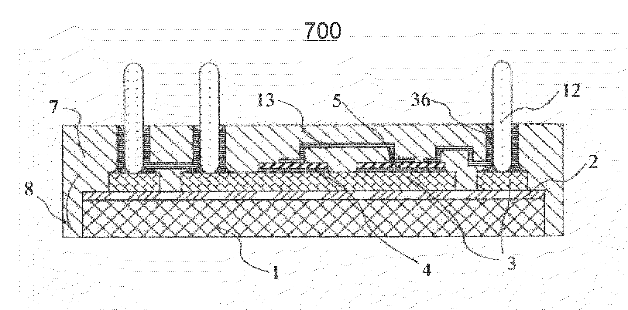
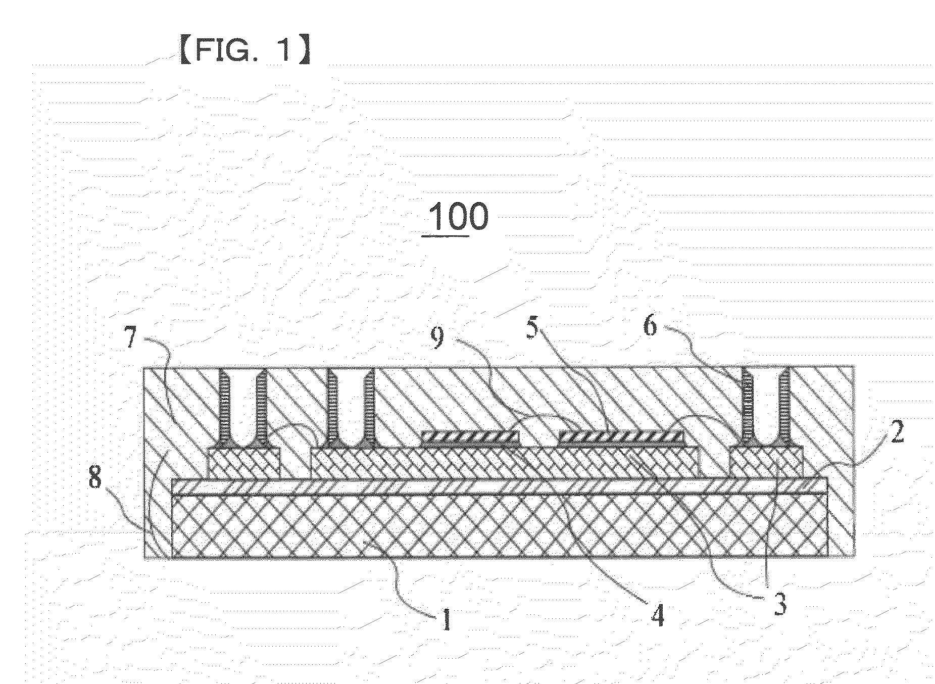
[0029]FIG. 1 is a schematic cross-sectional view showing a power semiconductor device according to the first embodiment of the present invention.
[0030]As shown in FIG. 1, in a power semiconductor device 100 of the present embodiment, a resin insulation layer 2 that is a high thermal conductive insulation layer is provided on one surface of a metal plate 1 that acts as a metal heat sink for dissipating heat of the power semiconductor device 100. A surface of the resin insulation layer 2 has a metallic foil wiring pattern 3 provided thereon, which surface is opposite to a surface, of the resin insulation layer 2, joined to the metal plate 1.
[0031]That is, the metal plate 1, the resin insulation layer 2 and the wiring pattern 3 constitute a metal circuit substrate 8. Power semiconductor elements 5 and cylindrical external terminal communication sections 6 are joined, by solder 4, to the wiring pattern 3. In particular, the cylindrical external terminal communication sections 6 are prov...
second embodiment
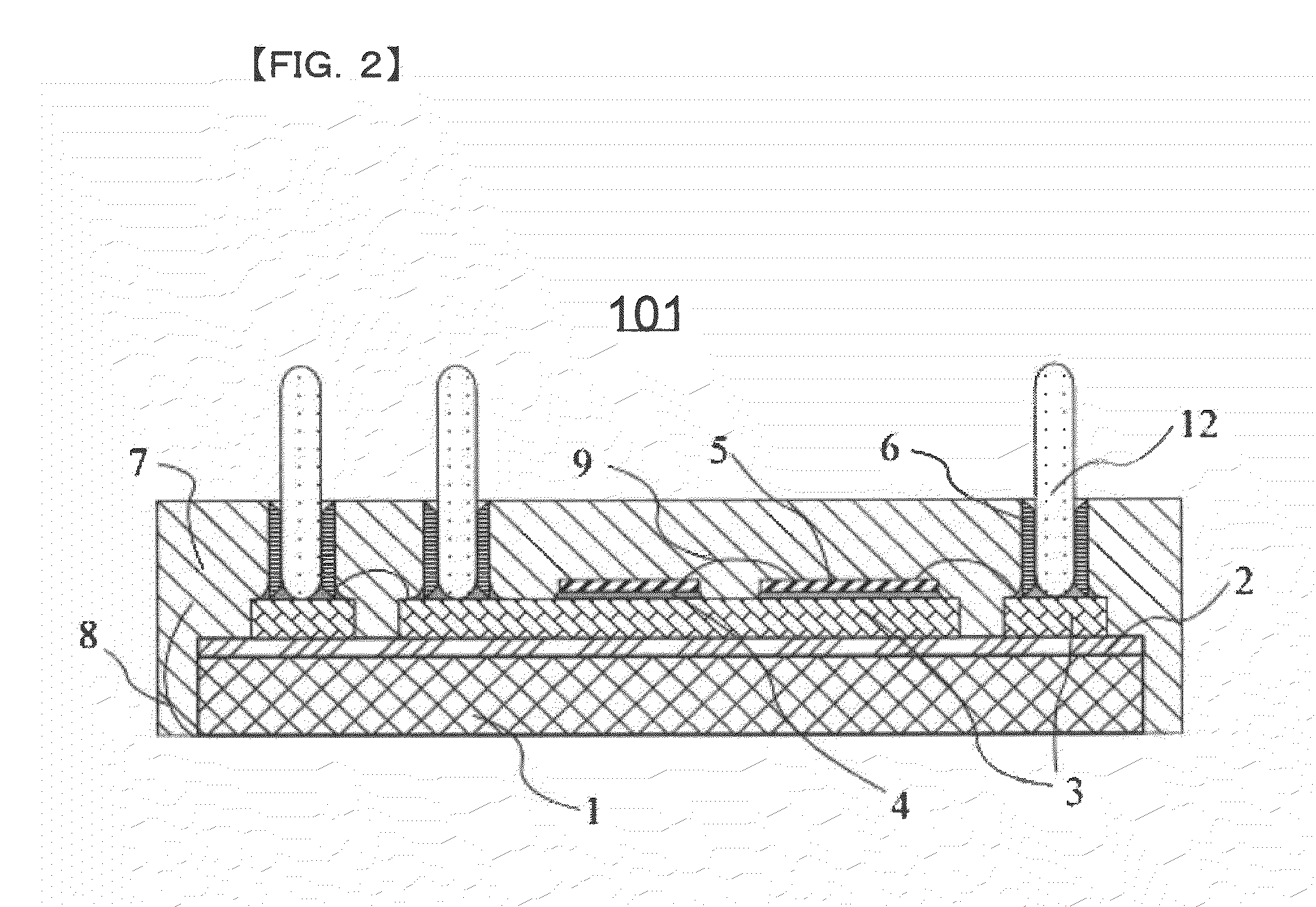
[0069]FIG. 4 is a schematic cross-sectional view of an area encompassing a cylindrical external terminal communication section provided in a power semiconductor device according to the second embodiment of the present invention.
[0070]FIG. 4 shows that an external terminal is inserted into the cylindrical external terminal communication section of the power semiconductor device.
[0071]As shown in FIG. 4, a power semiconductor device 200 of the present embodiment is the same as the first embodiment except that cylindrical external terminal communication sections 16 each having projections and depressions on the outer side surface thereof, are used. The height, from the bottom of the depressions of each cylindrical external terminal communication section 16, of the top of the projections is preferred to be 10 to 100 μm.
[0072]The power semiconductor device 200 of the present embodiment provides the same effects as those of the power semiconductor device 100 of the first embodiment. In ad...
third embodiment
[0073]FIG. 5 is a schematic cross-sectional view of an area encompassing a cylindrical external terminal communication section provided in a power semiconductor device according to the third embodiment of the present invention.
[0074]FIG. 5 shows that an external terminal is inserted into the cylindrical external terminal communication section of the power semiconductor device.
[0075]As shown in FIG. 5, a power semiconductor device 300 of the present embodiment is the same as the first embodiment except that portions of the wiring pattern 3, to which portions the cylindrical external terminal communication sections 6 are joined, are each provided with a groove 10 for mounting a cylindrical external terminal communication section thereon.
[0076]The power semiconductor device 300 of the present embodiment provides the same effects as those of the power semiconductor device 100 of the first embodiment. In addition, since the wiring pattern 3 is provided with the grooves 10 for mounting th...
PUM
 Abstract
Description
Claims
Application Information