Hybrid dielectric/surface plasmon polariton waveguide with grating coupling

a surface plasmon polariton and waveguide technology, applied in the field of waveguides, can solve the problems of low efficiency, dramatic loss, and decrease in propagation length, and achieve the effects of effective energy transfer, easy fabrication, and longer propagation rang

Inactive Publication Date: 2010-01-21
COLORADO SCHOOL OF MINES
View PDF17 Cites 25 Cited by
  • Summary
  • Abstract
  • Description
  • Claims
  • Application Information

AI Technical Summary

Benefits of technology

[0008]When the hybrid waveguide is multi-mode, embodiments of the present invention provide for effectively transferring energy back and forth between being concentrated in the dielectric waveguide and near the metal. This improves on standard SPP modes, yielding longer range propagation along with high intensity near the metal surface at decisive locations. For areas where very long ranges are required, the metal may be removed to make the range of the mode virtually infinite (limited by surface roughness).
[0009]Combining a grating with the hybrid waveguide provides one efficient and easily fabricated method for scattering light into the mode. This grating may have a rectangular profile, triangular profile, sinusoidal, or any other kind of profile to tune coupling efficiency. Simulations of designs have demonstrated 85% of the theoretical maximum of light transfer into the mode over a large collection area, which represents an extreme gain over conventional grating coupling of light into conventional SPP modes. Moreover, the utilization of two gratings to form a resonant cavity that further focuses the light to high intensity has been studied and can be achieved.
[0010]SPP waveguide designs utilized in accordance with at least some embodiments of the present invention partially overcome the problem that as the field is concentrated losses go up and propagation lengths go down. This improvement may be realized by decoupling the energy away from the metal surface in a dielectric waveguide with a “cladding” region between the metal and the dielectric waveguide. Depending on the thickness of the cladding region and dielectric waveguide, and for polarization states where the magnetic field is parallel to the surfaces, either a single mode hybrid waveguide or a multi-mode hybrid waveguide can be formed. In the case of a multi-mode hybrid waveguide, the energy can be catered to pass between being concentrated in the dielectric waveguide core and being concentrated at the metal surface. Therefore, at certain locations a high intensity of energy is concentrated at the metal surface, but the average intensity in the metal is lower than other designs leading to lower loss and longer propagation.
[0011]In addition, the efficiency of coupling light into the hybrid dielectric / SPP waveguide structure may be improved over prior art waveguides. Rather, in the various embodiments of the present invention, light very effectively couples in, making the design of these embodiments superior with respect to efficiency. Moreover, the mirrors utilized in accordance with embodiments of the present invention are very effective in reflecting energy back into the mode with lower diffractive loss as mentioned above.

Problems solved by technology

However, all of these waveguides retain the simple problem that as the field is concentrated, it is concentrated most at the metal, and hence the losses increase dramatically and the propagation lengths accordingly decrease.
However, for these designs, the efficiency is low because the grating meant to couple light into the mode almost as effectively couple light back out of the mode.
Gratings have been used with standard SPP modes as Bragg mirrors, but these designs have significant losses due to diffraction.

Method used


Image

  • Hybrid dielectric/surface plasmon polariton waveguide with grating coupling
  • Hybrid dielectric/surface plasmon polariton waveguide with grating coupling
  • Hybrid dielectric/surface plasmon polariton waveguide with grating coupling

Examples


Embodiment Construction

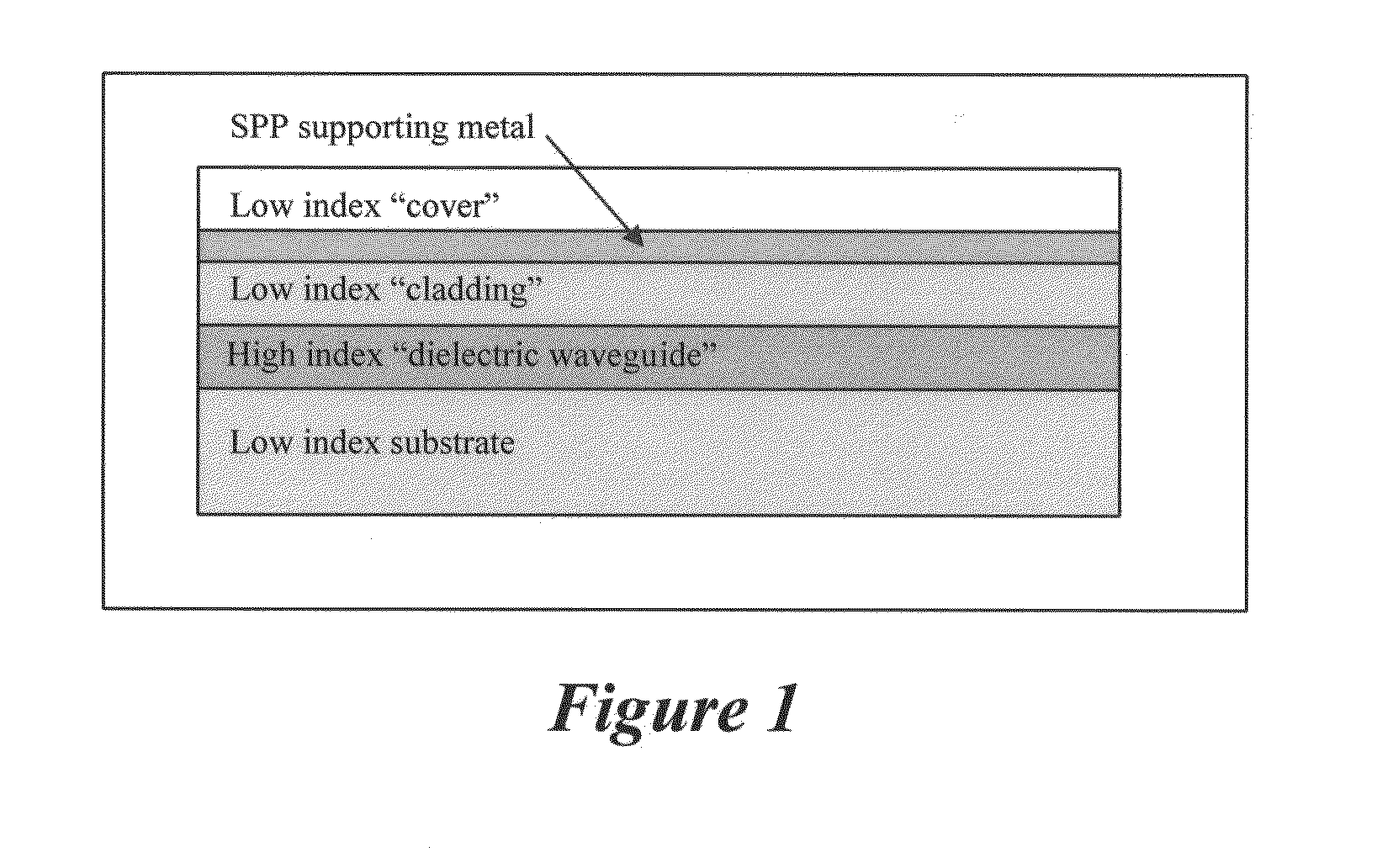
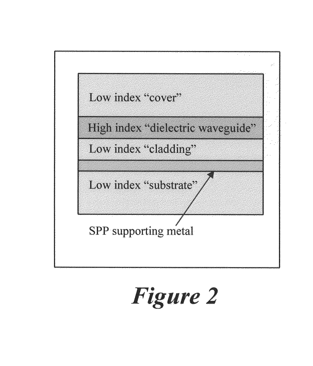
[0030]FIG. 1 shows components of the dielectric / SPP waveguide structure in accordance with at least some embodiments of the present invention:[0031]1) A bulk material (called substrate in the figure).[0032]2) A “dielectric waveguide” layer made of material with higher index than the substrate.[0033]3) A “cladding” layer with index lower than the dielectric waveguide layer.[0034]4) A metal layer (also referred to as the SPP layer) that is a good conductor over the spectral range of interest. This can be made very thin in order to increase the range of the surface plasmon mode, or may be made thick to confine propagation to one side of the metal.[0035]5) A “cover” layer typically of index lower than the dielectric waveguide layer. If the metal layer is thick enough that the SPP mode is one sided, it doesn't matter what the index of this layer is; if the metal is thin to decrease metallic losses, then the index should be lower than the dielectric waveguide layer. This could be air (no ...


PUM


Abstract

The present invention provides a hybrid dielectric / SPP waveguide that can form either a single mode, single polarization waveguide, or a multi-mode waveguide. When multi-mode, this invention effectively transfers energy back and forth between the dielectric waveguide and metal surface. This improves on standard SPP modes, yielding longer range propagation along with high intensity near the metal surface at decisive locations. When single-mode, this hybrid waveguide allows for control of propagation and confinement for applications such as telecommunications optics integrated on silicon microchips. Gratings may be patterned in the metal for coupling light into and out of the modes or for use as mirrors in the mode. For areas where very long ranges are required, a metal grating may be used to couple light into the mode, but then the metal may be removed in other regions and make the range of the mode virtually infinite (limited by surface roughness).

Description

CROSS-REFERENCE TO RELATED APPLICATION[0001]This Application claims the benefit of U.S. Provisional Application No. 61 / 059,016, filed Jun. 5, 2008, the entire disclosure of which is hereby incorporated herein by reference.[0002]The U.S. Government has a paid-up license in this invention and the right in limited circumstances to require the patent owner to license others on reasonable terms as provided for by the terms of DMI-0522281 awarded by the National Science Foundation and FA9550-06-1-0548 awarded by the Air Force Office of Scientific Research.FIELD OF THE INVENTION[0003]The invention generally related to waveguides and more particularly to Surface Plasmon Polariton (SPP) waveguides.BACKGROUND OF THE INVENTION[0004]Many waveguide designs have been used in an attempt to create a very long-range mode that has low losses while maintaining the ability to have a high signal near a metal surface at a predetermined location. More specifically, various surface plasmon polariton (SPP) ...

Claims


Application Information

Patent Timeline
Patent Type & Authority Applications(United States)
IPC IPC(8): G02B6/34G02B6/10B05D5/06
CPCB82Y20/00G02B6/124G02B6/1226
Inventor FLAMMER, P. DAVID
Owner COLORADO SCHOOL OF MINES
Why Eureka
Try Eureka