Multi-column electron beam exposure apparatus and multi-column electron beam exposure method

an electron beam and exposure method technology, applied in the field of electron beam exposure apparatus and electron beam exposure method, can solve the problems of marked reduction of design flexibility and variation in the width of the exposure pattern, and achieve the effect of improving the connection accuracy of the pattern

Active Publication Date: 2010-01-28
ADVANTEST CORP
View PDF2 Cites 14 Cited by
  • Summary
  • Abstract
  • Description
  • Claims
  • Application Information

AI Technical Summary

Benefits of technology

[0013]The present invention has been made in consideration of the problems in the prior art. An object of the present invention is to provide a multi-column electron beam exposure apparatus and a multi-column electron beam exposure method which achieve improved connection accuracy of patterns across column cells in the multi-column electron beam exposure apparatus.
[0017]In the present invention, the beam property is adjusted so that the beam properties of the electron beams emitted in the plurality of column cells may be approximately identical to each other. One column cell is selected among the plurality of column cells. By using the electron beam emitted from an electron gun of the column cell as the reference beam, the electron beams of the other column cells are adjusted so as to have a beam property approximated to the beam property of this reference beam. Thereby, the beam properties of the electron beams emitted in the plurality of column cells become approximately identical. Thus, it becomes possible to prevent shifting of an irradiation position or prevent varying of the pattern width, even when a pattern continuing across column cells is exposed. Accordingly, precise pattern exposure is attained.
[0019]In the present invention, a plurality of electron-beam-property detecting devices are used for detection of beam properties, of a same kind, of the electron beams used in the plurality of column cells. Each electron-beam-property detecting device detects the beam properties of the electron beams of the column cell group which has a pre-determined number of the plurality of column cells. The column cell groups have a column cell in common, and the beam properties of the electron beams of the other column cells in the column cell group are detected and adjusted on the basis of the beam property of the electron beam of the common column cell. This makes the beam properties of the electron beams used in all the column cells approximately identical. Even when a pattern extending across column cells is formed, the beam properties, such as the irradiation position, intensity, and the like of the electron beam, are identical among the column cells. Accordingly, improvement in the connection accuracy of the patterns is possible.
[0020]Moreover, since the properties of the electron beams used in the plurality of column cells is measured using the electron-beam-property detecting device located at a position close to those column cells, the movement range of the wafer stage moved in order to measure the beam properties is made smaller. Accordingly, deterioration of moving accuracy of the wafer stage is prevented, and in addition, a large space provided for the wafer stage movement is no longer necessary, thereby attaining miniaturization of the apparatus.

Problems solved by technology

/ b>. In this manner, there occurs a case where the width of the exposure pattern varies from area to area and a desired exposure pattern may not be obta
ined. Moreover, a position to be exposed may shift, and the pattern may be separated at
However, when the design is made taking positions of multiple column cells into consideration, the design flexibility is markedly reduced.

Method used


Image

  • Multi-column electron beam exposure apparatus and multi-column electron beam exposure method
  • Multi-column electron beam exposure apparatus and multi-column electron beam exposure method
  • Multi-column electron beam exposure apparatus and multi-column electron beam exposure method

Examples


first embodiment

(1) First Embodiment

Configuration of Multi-Column Electron Beam Exposure Apparatus

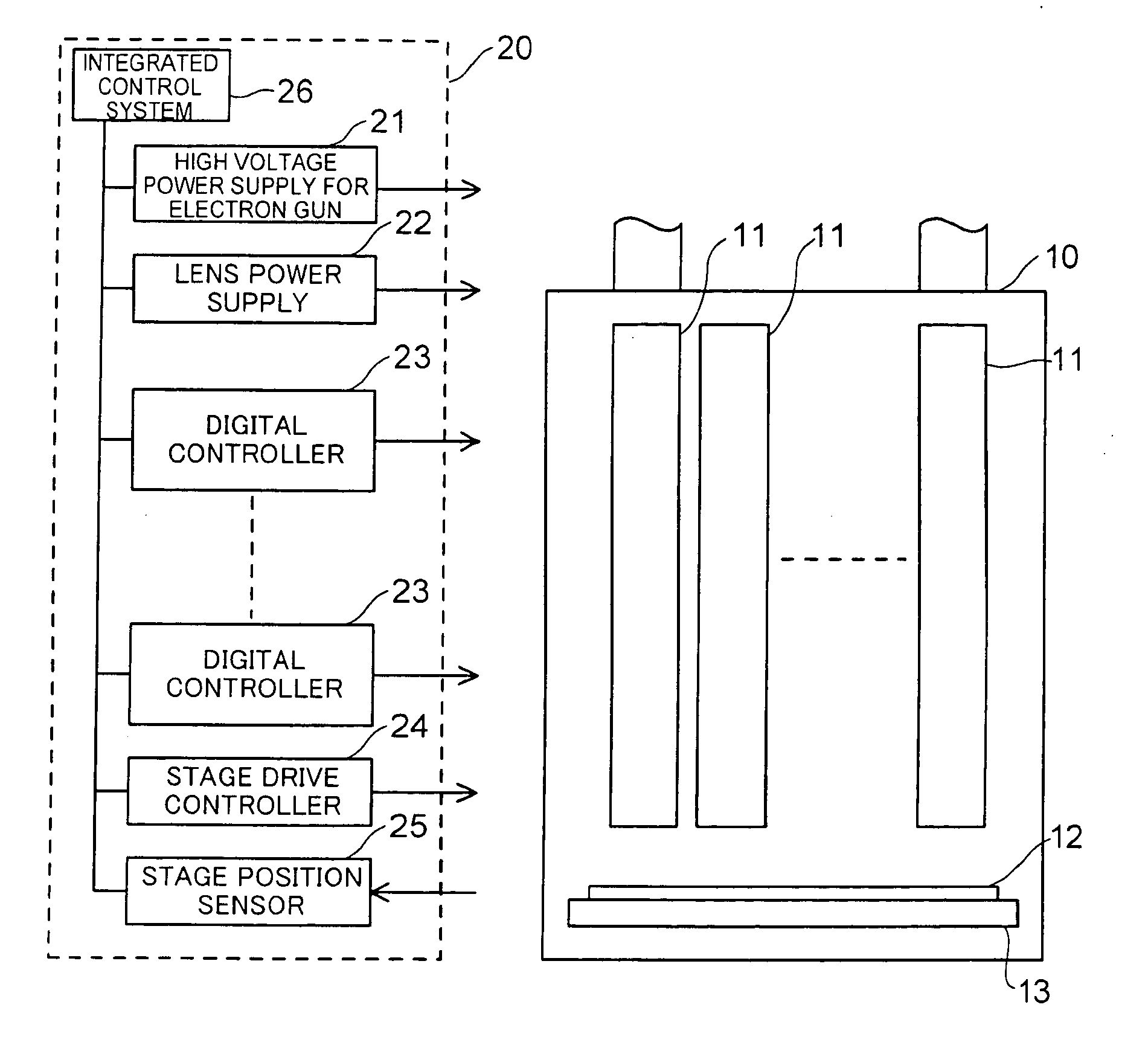
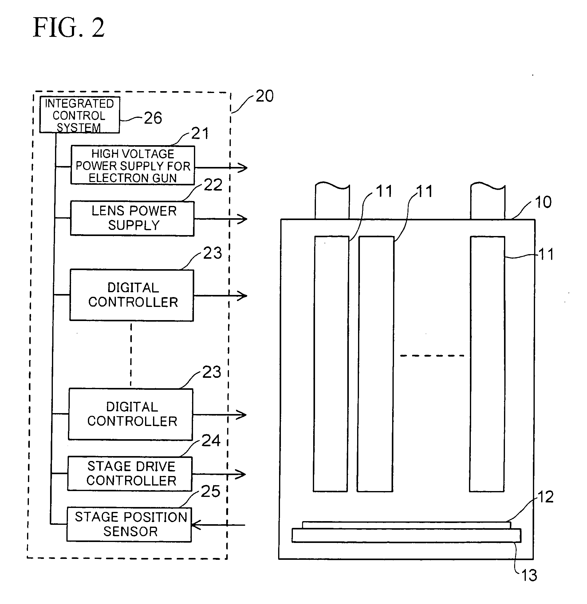
[0033]FIG. 2 is a schematic configuration diagram of a multi-column electron beam exposure apparatus according to the present embodiment. The multi-column electron beam exposure apparatus is mainly divided into an electron beam column 10 and a controller 20 which controls the electron beam column 10. Out of these, the electron beam column 10 includes multiple (for example, 16) identical column cells 11 to form the entire column. Every column cell 11 is formed of the same unit which will be described later. Below the column cells 11, a wafer stage 13 is disposed, with a, for example, 300-mm wafer 12 being mounted on the wafer stage 13.

[0034]On the other hand, the controller 20 includes a high voltage power supply 21 for electron gun, a lens power supply 22, a digital controller 23, a stage drive controller 24, and a stage position sensor 25. Out of these, the high voltage power supply 21 for electron gu...

second embodiment

(2) Second Embodiment

[0112]In the first embodiment, the properties of the electron beams in all the column cells are measured using one electron-beam-property detecting device for the beam property of the same kind, and are adjusted so as to be approximated to the reference beam properties.

[0113]Unlike the first embodiment, in the present embodiment, in order to approximate the electron beam properties of all the column cells to the reference beam properties, multiple electron-beam-property detecting devices are used.

[0114]Note that a multi-column electron beam exposure apparatus used in the present embodiment has the same configuration as that of the first embodiment, and therefore description thereof will be omitted.

[0115]Hereinafter, description will be given on a method for approximating the electron beam properties of all the column cells to the reference beam properties by using the multiple electron-beam-property detecting devices.

[0116]FIG. 9 shows some of the column cells w...


PUM


Abstract

A multi-column electron beam exposure apparatus includes: a plurality of column cells; a wafer stage including an electron-beam-property detecting unit for measuring an electron beam property; and a controller for measuring beam properties of electron beams used in all the column cells by using the electron-beam-property detecting unit, and for adjusting the electron beams of the respective column cells so that the properties of the electron beams used in the column cells may be approximately identical. The electron beam property may be any of a beam position, a beam intensity, and a beam shape of the electron beam to be emitted. The electron-beam-property detecting unit may be a chip for calibration with a reference mark formed thereon or a Faraday cup.

Description

CROSS-REFERENCE TO RELATED APPLICATIONS[0001]This application is a continuation of prior International Patent Application No. PCT / JP2007 / 056246, filed Mar. 26, 2007, the entire contents of which are incorporated herein by reference.BACKGROUND OF THE INVENTION[0002]1. Field of the Invention[0003]The present invention relates to an electron beam exposure apparatus and an electron beam exposure method. Particularly, it relates to a multi-column electron beam exposure apparatus and a multi-column electron beam exposure method which are suitable for exposing process with multiple column cells.[0004]2. Description of the Prior Art[0005]In prior art electron beam exposure apparatuses, a variable rectangular opening or multiple stencil mask patterns are provided to a stencil mask, and a certain pattern of the opening or a certain stencil mask pattern is selected by beam deflection and is exposed and transferred onto a wafer. Although multiple mask patterns are prepared in an electron beam e...

Claims


Application Information

Patent Timeline
Patent Type & Authority Applications(United States)
IPC IPC(8): H01J37/30
CPCB82Y10/00B82Y40/00G03F7/2059H01J37/3045H01J2237/24542H01J37/3177H01J2237/24507H01J2237/24521H01J2237/24535H01J37/3174
Inventor YAMADA, AKIOYASUDA, HIROSHINAKANO, MITSUHIROKIUCHI, TAKASHI
Owner ADVANTEST CORP
Why Eureka
Try Eureka