
Method and device of diamond like carbon multi-layer doping growth

a multi-layer, diamond-like technology, applied in the direction of photovoltaic energy generation, electrical equipment, climate sustainability, etc., can solve the problems of low-cost, stable and highly efficient solar cells that are yet to be commercialized, and relatively few publications on the pv properties of c/si hetero-structures, etc., to optimize thermal response, optimize electron mobility, and optimize spectral response

Active Publication Date: 2010-02-04
MAHRIZE MOSHE
View PDF9 Cites 6 Cited by
  • Summary
  • Abstract
  • Description
  • Claims
  • Application Information

AI Technical Summary

Benefits of technology

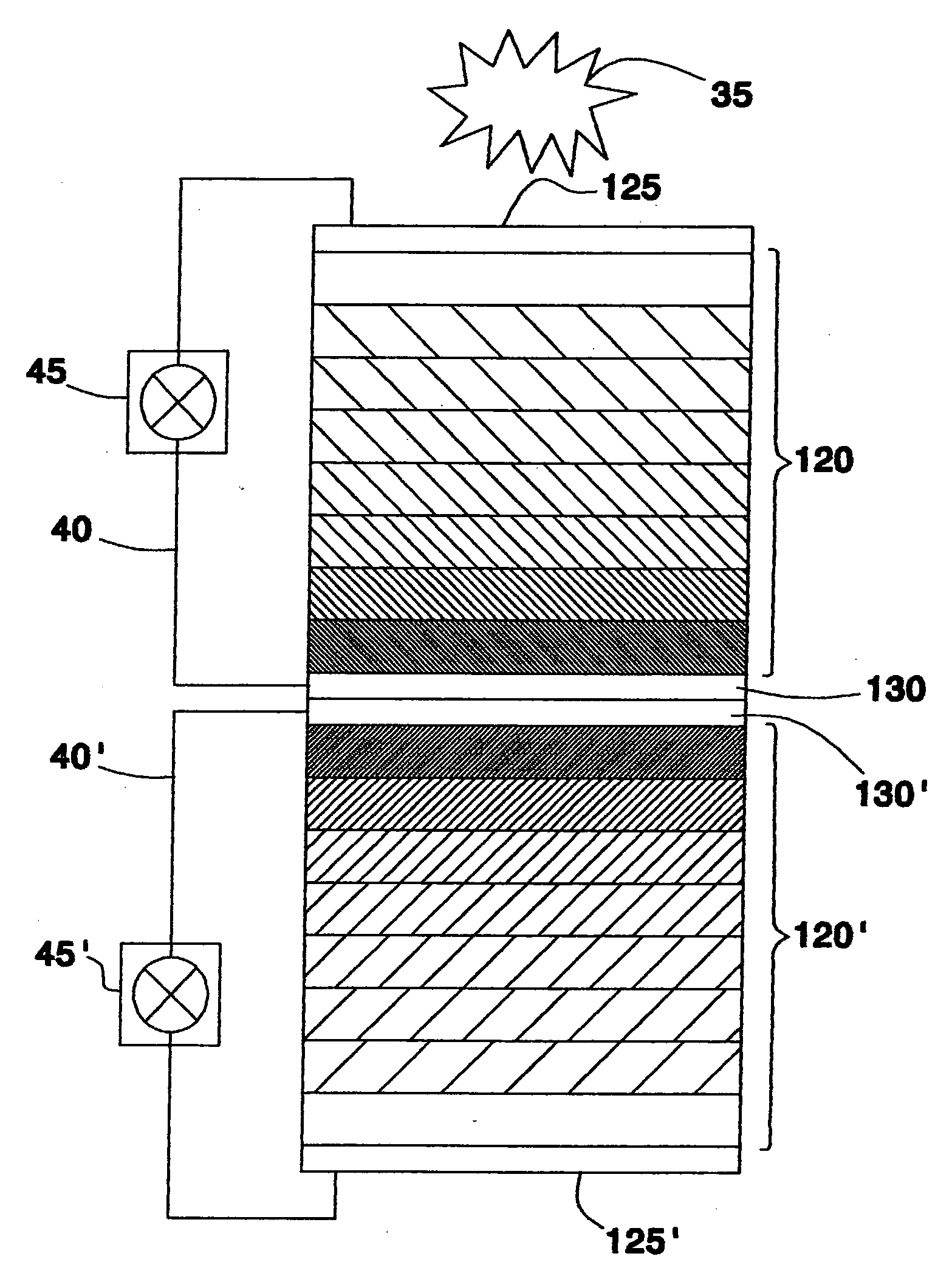
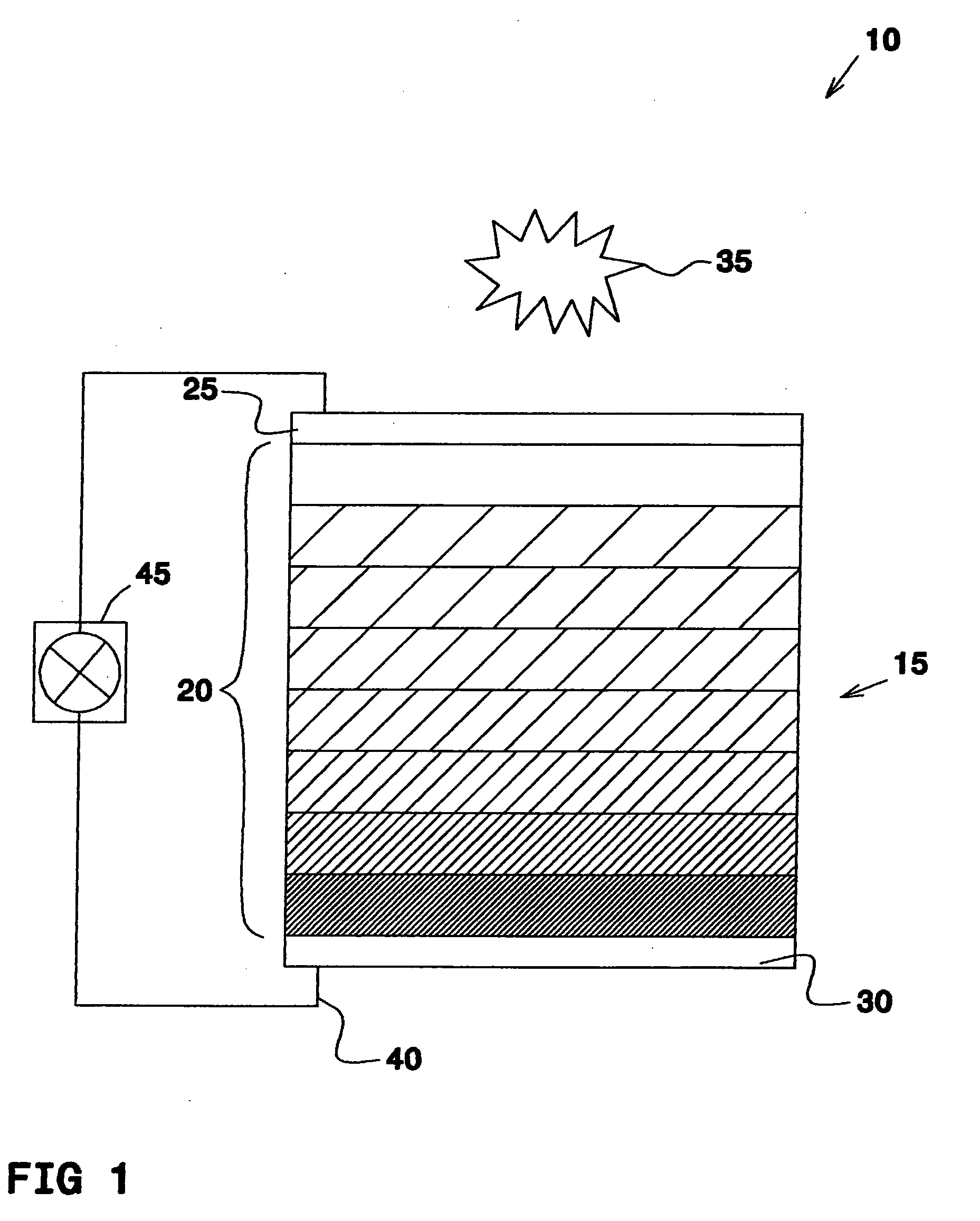
[0012]According to the teachings of the present invention there is provided, a method of a:DLC multi-layer doping growth comprising the steps of: forming a plurality of a:DLC layers in one process, thereby creating a plurality of successively connected PIN junctions, starting from a first junction and ending in a last junction, respective PIN junctions having p-type, n-type, and intrinsic layers; varying the sp2 / sp3 ratio of at least the respective p-type and n-type layers and doping with at least silver to enhance electron mobility in respective PIN junctions; and connecting the plurality of a:DLC layers between electrodes at the first side and the second side to create a device having optimized spectral response to being oriented to a light source. Preferably, the sp3 / sp2 ratio is varied in a:DLC layers with the ratio ranging from between substantially 4.0 eV or more in a:DLC layers closest to the light source to substantially 0.60 in a:DLC layers furthest from the light source. Most preferably, doping of a:DLC layers with at least silver is performed to yield a controlled photovoltaic response from the first junction to the last junction. Typically, wherein the optimized spectral response yields optimized energy efficiency of the device. Most typically, the optimized spectral response further comprises focusing incident light onto the device. Preferably, the device is a photovoltaic cell. Typically the device is part of an integrated circuit. Most typically, the device is a solar cell.
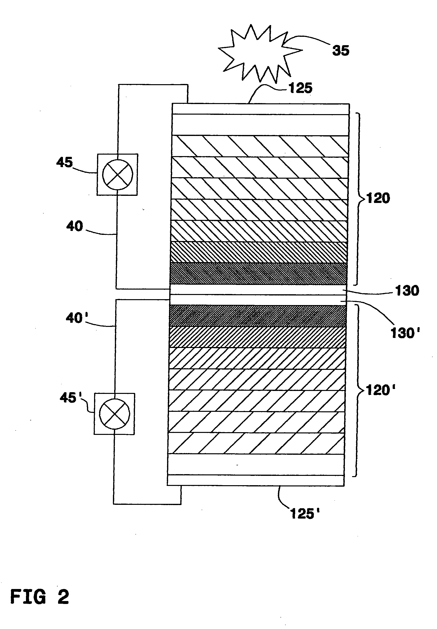
[0014]There is further provided a method of enhanced a:DLC multi-layer doping growth comprising the steps of: forming a first plurality of a:DLC layers in one process, thereby creating a plurality of successively connected PIN junctions, starting from a first junction and ending in a last junction, respective PIN junctions having p-type, n-type, and intrinsic layers; varying the sp3 / sp2 ratio of at least the respective p-type and n-type layers and doping with at least silver to enhance electron mobility in respective PIN junctions; fabricating an second plurality of a:DLC layers according to steps a and b; connecting the first plurality of a:DLC layers between electrodes at the layers' respective first side and second side and connecting the second plurality of a:DLC layers between electrodes at the layers' respective first side and second side; and connecting the respective electrodes of the respective second sides of the two pluralities of a:DLC layers to create a device having optimized spectral response to being oriented to a light source and an optimized thermal response. Preferably, the optimized spectral response further comprises focusing incident light onto the device. Most preferably, the device is a solar cell. Typically, the device is part of an integrated circuit.

Problems solved by technology

Although silicon and compound-semiconductor-based solar cells have dominated the market for the last few decades, low-cost, stable and highly efficient solar cells are yet to be commercially realized due to high material and production costs.
However, relatively few publications are available on the PV properties of C / Si hetero-structures.

Method used


Image

  • Method and device of diamond like carbon multi-layer doping growth
  • Method and device of diamond like carbon multi-layer doping growth
  • Method and device of diamond like carbon multi-layer doping growth

Examples


Embodiment Construction

[0018]The present invention is a method and device of amorphous diamond like carbon multi-layer doping growth, and in particular, it concerns a process of forming a variable structure with mix control (sp3 / sp2 ratio) to obtain a large spectrum energy gap for multi-junction photovoltaic cells and other applications.

[0019]The principles method for amorphous diamond like carbon multi-layer doping growth according to the present invention may be better understood with reference to the drawings and the accompanying description.

[0020]In the specification and the claims hereinbelow, the following terms are defined.

[0021]“Amorphous Diamond-like carbon” (alternatively “a:DLC” and / or “a-C:H”) is intended to mean a hydrogenated carbonaceous material having carbon atoms as the majority element, with a substantial amount of such carbon atoms bonded in distorted tetrahedral coordination. a:DLC can typically be formed by PVD processes, although CVD or other processes could be used such as vapor de...


PUM

PropertyMeasurementUnit
work functionaaaaaaaaaa
thicknessesaaaaaaaaaa

Abstract

A method of a:DLC multi-layer doping growth comprising the steps of: forming a plurality of a:DLC layers in one process, thereby creating a plurality of successively connected PIN junctions, starting from a first junction and ending in a last junction, respective PIN junctions having p-type, n-type, and intrinsic layers; varying the sp3 / sp2 ratio of at least the respective p-type and n-type layers and doping with at least silver to enhance electron mobility in respective PIN junctions; and connecting the plurality of a:DLC layers between electrodes at the first side and the second side to create a device having optimized spectral response to being oriented to a light source.

Description

[0001]This application claims priority from U.S. Provisional Patent Application No. 60 / 901,033 filed 13 Feb. 2007, incorporated herein by reference.FIELD AND BACKGROUND OF THE INVENTION[0002]The present invention relates to a method and device of amorphous diamond like carbon thin multi-layer doping growth, and in particular, it concerns a process of forming a variable structure with mix control (sp3 / sp2 ratio) to obtain a large spectrum energy gap for multifunction photovoltaic and thermal solar cells and other applications.[0003]In recent years, amorphous Diamond Like Carbon (a:DLC, or a-C:H) films have been developed. a:DLC films are easier to deposit on large substrate areas (such as plastic), at low temperature, as compared to CVD diamond-like carbon (DLC) films. The unique properties of a:DLC films are similar to those of single crystal bulk diamonds, including: high hardness, low friction coefficient, chemical inertness, infrared transparency, high electrical resistivity, and...

Claims


Application Information

Patent Timeline
Patent Type & Authority Applications(United States)
IPC IPC(8): H01L31/04H01L31/0312H01L31/18
CPCH01L31/022466H01L31/028H01L31/0288Y02E10/548H01L31/076H01L31/1884H01L31/202H01L31/03762Y02P70/50
Inventor MAHRIZE, MOSHE
Owner MAHRIZE MOSHE
Learn More