Perovskite/N-type TOPCon/perovskite laminated solar cell and preparation method thereof

A solar cell and perovskite technology, applied in the field of solar cells, can solve the problems of high back reflectivity, absorption, and low light utilization rate, and achieve the effects of convenient and simple preparation methods, improved spectral response, and improved light absorption performance

Active Publication Date: 2020-08-11
TAIZHOU ZHONGLAI PHOTOELECTRIC TECH CO LTD
View PDF4 Cites 4 Cited by
  • Summary
  • Abstract
  • Description
  • Claims
  • Application Information

AI Technical Summary

Problems solved by technology

However, at present, many cells use double-sided light input to increase the incident light to increase the photocurrent. In order to increase the incident light on the back, many solar cell power stations use flat mirrors to supplement the light on the back. Full absorption; In addition, silicon solar cells are usually made of single-sided texture, the back reflectivity is high, and the light utilization rate is low

Method used


Image

  • Perovskite/N-type TOPCon/perovskite laminated solar cell and preparation method thereof
  • Perovskite/N-type TOPCon/perovskite laminated solar cell and preparation method thereof
  • Perovskite/N-type TOPCon/perovskite laminated solar cell and preparation method thereof

Examples


preparation example Construction

[0049] A kind of preparation method of perovskite / N type TOPCon / perovskite laminated solar cell of the present invention comprises the following steps:

[0050] (1), prepare p+ doped regions on both sides of the silicon substrate after the double-sided texturing treatment;

[0051] (2), any side of the silicon substrate treated in step (1) is put into an acidic solution for etching treatment, to remove the p+ doped region on the back side;

[0052] (3), preparing a tunnel oxide layer and an intrinsic amorphous silicon layer on the back side of the silicon substrate treated in step (2);

[0053] (4) Perform doping treatment on the intrinsic crystalline silicon layer of the silicon substrate treated in step (3), and clean it.

[0054] (5), performing rapid annealing treatment on the silicon substrate after step (4), to form a doped polysilicon film on the tunnel oxide layer; and remove the polysilicon winding on the front side of the silicon substrate;

[0055] (6), composite ...

Embodiment 1

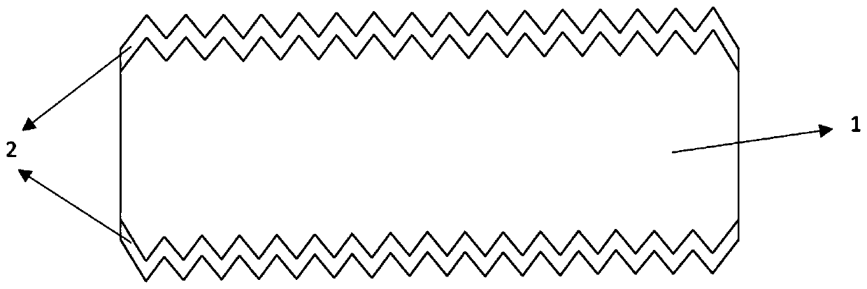
[0079] Step (1), select N-type silicon with a thickness of 150-170 μm, a resistivity of 0.3-2Ω·cm, and a size of 156.75mm×156.75mm as the substrate for double-sided texturing; On the silicon surface, boron tribromide is used as the boron source to prepare the double-sided p+ doped region 2, the diffusion temperature is 850-1000°C, the time is 50-80min, and the square resistance is 80-100Ω / sqr. The battery structure after completing this step is as follows: figure 1 shown.

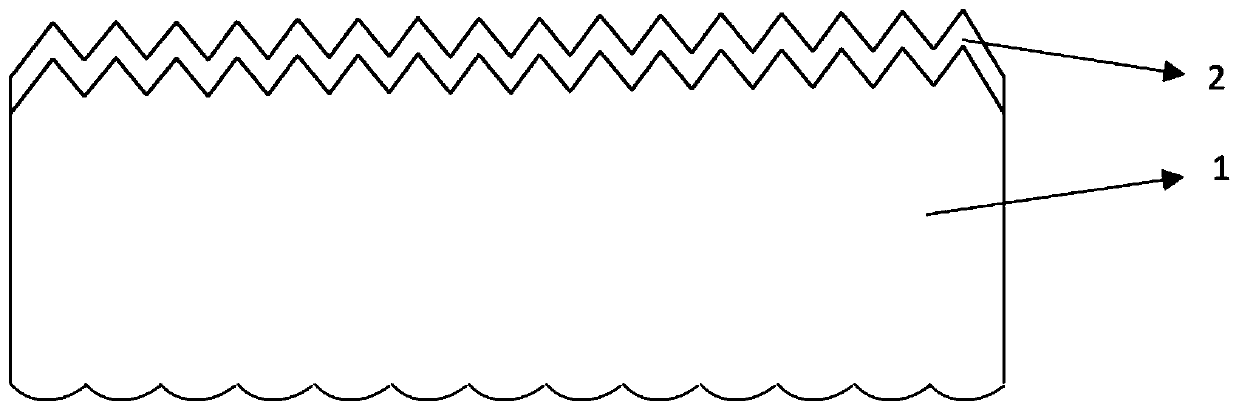
[0080] Step (2), select one side of the N-type silicon after double-sided boron diffusion into HF and HNO 3 , and H 2 SO 4 Etching treatment is carried out in the mixed solution to remove the p+ doped region 2 on the back side to obtain a smooth pyramid surface after etching, wherein, HF:HNO 3 :H 2 SO 4 :H 2 O=1:4:0.6:3, HF mass fraction 20%. The battery structure after completing this step is as follows figure 2 shown.

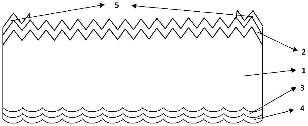
[0081] In step (3), an ultra-thin tunneling oxide layer 3 is prepared on th...

Embodiment 2

[0088] Step (1), select N-type silicon with a thickness of 150-170 μm, a resistivity of 0.3-2Ω·cm, and a size of 156.75mm×156.75mm as the substrate for double-sided texturing; On the silicon surface, boron tribromide is used as the boron source to prepare the double-sided p+ doped region 2, the diffusion temperature is 850-1000°C, the time is 50-80min, and the square resistance is 80-100Ω / sqr. The battery structure after completing this step is as follows: figure 1 shown.

[0089] Step (2), select one side of the N-type silicon after double-sided boron diffusion into HF and HNO 3 , and H 2 SO 4 Etching treatment is carried out in the mixed solution to remove the p+ doped region 2 on the back side to obtain a smooth pyramid surface after etching, wherein, HF:HNO 3 :H 2 SO 4 :H 2 O=1:4:0.6:3, HF mass fraction 20%. The battery structure after completing this step is as follows figure 2 shown.

[0090] In step (3), an ultra-thin tunneling oxide layer 3 is prepared on th...


PUM

PropertyMeasurementUnit
thicknessaaaaaaaaaa
thicknessaaaaaaaaaa
thicknessaaaaaaaaaa

Abstract

The invention relates to a preparation method of a perovskite/N-type TOPCon/perovskite laminated solar cell and the perovskite/N-type TOPCon/perovskite laminated solar cell. The method comprises the following steps: (1) preparing p+ doped regions on two sides of a silicon substrate after double-side texturing; (2) etching one surface of the silicon substrate in an acidic solution to remove a p+ doped region on the back surface; (3) preparing a tunneling oxide layer and an intrinsic amorphous silicon layer on the back surface of the silicon substrate; and (4) carrying out doping treatment on the intrinsic crystal silicon layer of the silicon substrate, and cleaning. (5) annealing the silicon substrate to form a doped polycrystalline silicon film; removing the polycrystalline silicon windingdegree on the front surface; (6) preparing composite layers on the two sides of the silicon substrate; (7) sequentially preparing a front electron transport layer, a front perovskite absorption layerand a front hole transport layer on the front composite layer of the silicon substrate; sequentially preparing a back hole transport layer, a back perovskite absorption layer and a back electron transport layer on the back composite layer of the silicon substrate; and (8) preparing metal electrodes on the two sides of the silicon substrate.

Description

technical field [0001] The invention relates to the technical field of solar cells, in particular to a method for preparing a perovskite / N-type TOPCon / perovskite laminated solar cell and the cell. Background technique [0002] As a new type of solar cell, perovskite solar cells have the advantages of low production cost, simple preparation process, high electrical mobility, and large light absorption coefficient. Since 2009, its conversion efficiency has jumped from the initial 3.8% to 25.2%, and the growth rate is breathtaking. However, there is still a problem with perovskite solar cells, which is that their spectral response region does not match the solar spectrum. The perovskite solar cell has a band gap of 1.5eV, and cannot absorb ultraviolet light with a wavelength of less than 400nm and near-infrared light with a wavelength greater than 800nm. Therefore, light that accounts for nearly half of the solar spectrum is not utilized by perovskite solar cells, which greatl...

Claims


Application Information

Patent Timeline
Patent Type & Authority Applications(China)
IPC IPC(8): H01L51/48H01L31/20H01L31/0747H01L51/42H01L51/44H01L27/28H01L27/30
CPCH01L31/202H01L31/0747H10K19/20H10K30/57H10K71/10H10K30/35H10K30/87H10K30/30Y02E10/549Y02P70/50
Inventor 崔义乾吴伟梁乔振聪马丽敏陈浩刘志锋林建伟
Owner TAIZHOU ZHONGLAI PHOTOELECTRIC TECH CO LTD
Why Eureka
Try Eureka