Heterojunction solar cell of inclined metal contact structure based on N type silicon wafer

A metal contact, solar cell technology, applied in circuits, photovoltaic power generation, electrical components, etc., can solve the problems of amorphous silicon thin film solar cell application limitations, many thin film defects, low conversion efficiency and other problems

Inactive Publication Date: 2012-10-03
ZHEJIANG JINKO SOLAR CO LTD
View PDF5 Cites 5 Cited by
  • Summary
  • Abstract
  • Description
  • Claims
  • Application Information

AI Technical Summary

Problems solved by technology

However, hydrogenated amorphous silicon ( ) film has many defects, resulting in low conversion efficiency, and its conversion efficiency will continue to decrease with the time of illumination, which limits the application of amorphous silicon thin film solar cells

Method used


Image

  • Heterojunction solar cell of inclined metal contact structure based on N type silicon wafer
  • Heterojunction solar cell of inclined metal contact structure based on N type silicon wafer

Examples


Embodiment 1

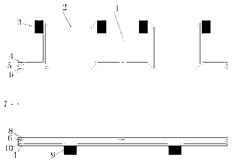
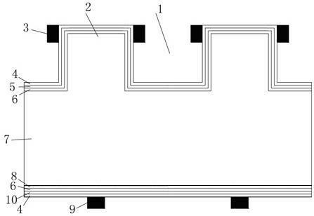
[0018] like figure 1 As shown, a heterojunction solar cell based on an N-type silicon wafer inclined metal contact structure, including an N-type single silicon wafer substrate 7. Battery positive electrode 3. Groove 1. Intrinsic hydrogenated nano-silicon Thin film 6, P-type heavily doped hydrogenated nano-silicon Thin film 5, N-type heavily doped hydrogenated nano-silicon Thin film 10, N formed by diffusing phosphorus source + Heavy doping layer 8, transparent conductive film TCO 4, battery negative electrode 9. The N-type monocrystalline silicon substrate 7 Set groove 1 on the front (main light-receiving surface), and deposit a layer of intrinsic hydrogenated nano-silicon sequentially on the front Thin film 6, P-type heavily doped hydrogenated nano-silicon Film 5, in P-type heavily doped hydrogenated nano-silicon A layer of transparent conductive film TCO 4 is prepared on the film 5; the N-type single crystal silicon substrate 7 Phosphorus source diffused on t...

Embodiment 2

[0023] like figure 1 As shown, a heterojunction solar cell based on an N-type silicon wafer inclined metal contact structure, including an N-type single silicon wafer substrate 7. Battery positive electrode 3. Groove 1. Intrinsic hydrogenated nano-silicon Thin film 6, P-type heavily doped hydrogenated nano-silicon Thin film 5, N-type heavily doped hydrogenated nano-silicon Thin film 10, N formed by diffusing phosphorus source + Heavy doping layer 8, transparent conductive film TCO 4, battery negative electrode 9. The N-type monocrystalline silicon substrate 7 Set groove 1 on the front (main light-receiving surface), and deposit a layer of intrinsic hydrogenated nano-silicon sequentially on the front Thin film 6, P-type heavily doped hydrogenated nano-silicon Film 5, in P-type heavily doped hydrogenated nano-silicon A layer of transparent conductive film TCO 4 is prepared on the film 5; the N-type single crystal silicon substrate 7 Phosphorus source diffused on...

Embodiment 3

[0028] The positive electrode 3 of the battery is made by plating Ag on the N-type monocrystalline silicon substrate by vacuum evaporation. 7 Both sides inside the front groove 1. All the other are identical with embodiment 1.


PUM


Abstract

The invention relates to a heterojunction solar cell of an inclined metal contact structure based on an N type silicon wafer. The heterojunction solar cell of the inclined metal contact structure based on the N type silicon wafer comprises an N type mono-crystalline silicon base body, a positive electrode, a negative electrode, transparent conductive films and a plurality of film layers manufactured and formed on the front face and the back face of the N type mono-crystalline silicon base body, wherein each film layer manufactured and formed on the back face of the N type mono-crystalline silicon base body comprises an N<+> heavily-doped layer, forming N<+> / N high-low junctions; one layer of transparent conductive film is manufactured and formed on the outermost layer of each of the front face and the back face of the N type mono-crystalline silicon base body; a recess is arranged on the front face of the N type mono-crystalline silicon base body; the positive electrode of the cell is put in the recess; and the negative electrode of the cell is put on the back face of the N type mono-crystalline silicon base body. Generating no drastic light failure phenomenon of the heterojunction solar cell constituted by the routine P type crystalline silicon and the crystalline silicon of a non-crystalline silicon film, the heterojunction solar cell of the inclined metal contact structure based on the N type silicon wafer is better in spectral response, and further is greatly thinned; the shading area of grid lines is decreased from 6% to 1% of the routine silk-screen printing mode, so that the conversion efficiency of the solar cell is improved; and additionally, with the adoption of a low temperature production process, the production cost is reduced.

Description

technical field [0001] The invention relates to the technical field of semiconductor solar cells, in particular to a heterojunction solar cell based on an N-type silicon wafer inclined metal contact structure. Background technique [0002] In the 21st century, energy crisis and environmental pollution have become global problems that need to be solved urgently. The development of green energy has become one of the main methods to solve this crisis. Solar cells have the advantages of safety and environmental protection, so photovoltaic industry technology has become the goal of development of various countries. [0003] At present, traditional crystalline silicon solar cells use high-temperature processes in production, such as diffusion and sintering temperatures above 800°C, which easily lead to deformation and thermal damage of crystalline silicon wafers, and consume a lot of energy and cost. [0004] The grid lines of traditional heterojunction solar cells are directly ...

Claims


Application Information

Patent Timeline
Patent Type & Authority Applications(China)
IPC IPC(8): H01L31/0224H01L31/077
CPCY02E10/50Y02E10/547
Inventor 聂金艳涂宏波王学林梅晓东
Owner ZHEJIANG JINKO SOLAR CO LTD
Why Eureka
Try Eureka