Method for forming organic semiconductor thin film and method of manufacturing thin-film semiconductor device

a technology of organic semiconductor and thin film, which is applied in the direction of semiconductor devices, basic electric elements, electrical equipment, etc., can solve the problems of limited material selection freedom in printing formation of this type of organic semiconductor thin film, and achieve the effect of increasing the degree of selection freedom and increasing the selection of organic semiconductor materials

Inactive Publication Date: 2010-02-04
SONY CORP
View PDF3 Cites 10 Cited by
  • Summary
  • Abstract
  • Description
  • Claims
  • Application Information

AI Technical Summary

Benefits of technology

[0009]This type of method enables transcription onto a substrate by mixing an organic material enabling transcription even in an ink formed from an organic semiconductor material not enabling transcription from a printing plate. Consequently, in contrast to previous printing methods, transcription and formation of an organic semiconductor thin film is enabled on a substrate when using an organic semiconductor material not previously capable of use with printing methods for film formation. Furthermore the freedom of selection of organic semiconductor materials is increased with respect to the formation of organic semiconductor thin films.
[0010]The embodiment of the present invention as described above displays a high degree of freedom of selection with respect to organic semiconductor materials for the formation of organic semiconductor thin films by transcription and printing and, as a result, enables the manufacture of thin-film semiconductor devices displaying preferred properties by the application of printing methods.

Problems solved by technology

However the level of freedom of selection of materials in printing formation of this type of organic semiconductor thin film has been limited by the number of organic semiconductor materials which enable transcription and printing from a stamp plate.
However TIPS pentacene does not transcribe onto a device substrate in film formation applying printing method and therefore it is not used in pattern formation associated with printing methods.
Firstly an ink is prepared from a mixture of an organic semiconductor material which does not enable transcription from a printing plate to a substrate in an ink form dissolved in a solvent and an organic material enabling transcription which is in the same state.

Method used


Image

  • Method for forming organic semiconductor thin film and method of manufacturing thin-film semiconductor device
  • Method for forming organic semiconductor thin film and method of manufacturing thin-film semiconductor device
  • Method for forming organic semiconductor thin film and method of manufacturing thin-film semiconductor device

Examples


first embodiment

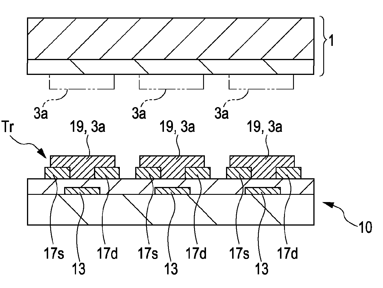
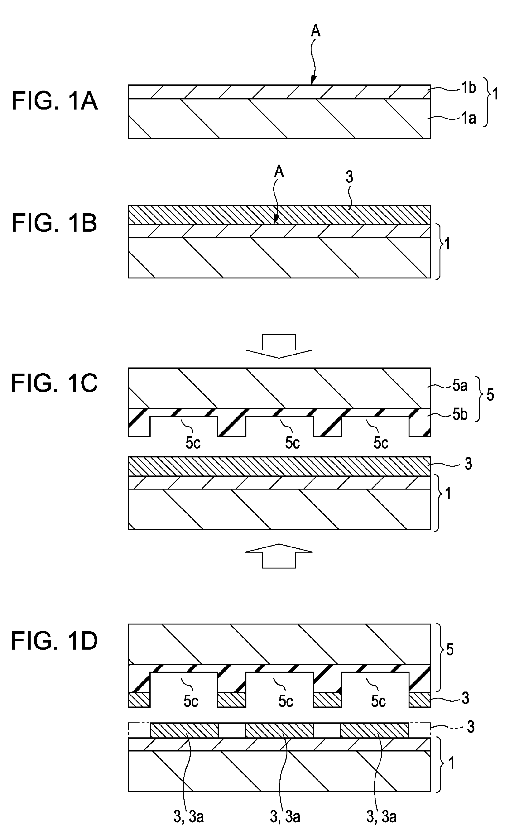
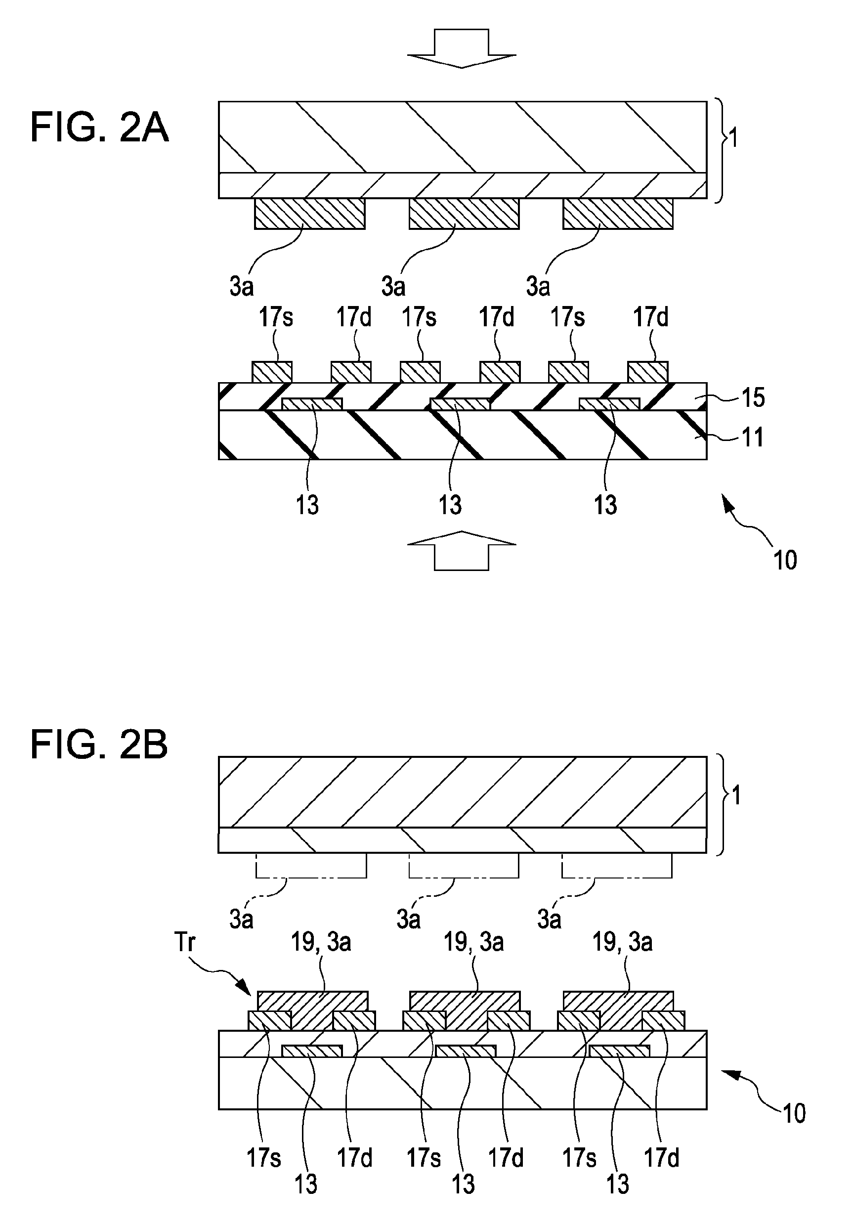
[0019]FIGS. 1A to 2B are sectional process views showing show a method of manufacture according to a first embodiment of the present invention. A method of forming an organic semiconductor thin film according to the first embodiment and a method of manufacturing a thin-film semiconductor device using the organic semiconductor thin film will be described hereafter making reference to FIGS. 1A to 2B. The first embodiment will describe the manufacture of a thin-film semiconductor device provided with a plurality of bottom-gate bottom-contact organic thin-film transistors.

[0020]Firstly a printing plate 1 is prepared as shown in FIG. 1A. The printing plate 1 may use a blanket layer 1b formed from liquid-resistant PDMA to cover a surface of a supporting substrate 1a with the surface side of the blanket layer 1b forming a liquid-resistant surface A.

[0021]Then as shown in FIG. 1B, a mixed ink layer 3 according to the embodiment of the present invention is coated and dried on the liquid-resi...

second embodiment

[0038]FIGS. 4A to 5B are sectional process views showing a method of manufacture according to a second embodiment of the present invention. A method of forming an organic semiconductor thin film according to the second embodiment and a method of manufacturing a thin-film semiconductor device using the organic semiconductor thin film will be described hereafter using FIGS. 4A to 5B. The second embodiment will describe the manufacture of a thin-film semiconductor device provided with a plurality of bottom-gate bottom-contact organic thin-film transistors in the same manner as the first embodiment.

[0039]Firstly a printing plate 1 is prepared as shown in FIG. 4A in the same manner as the first embodiment. The printing plate 1 includes a blanket layer 1b formed from liquid-resistant PDMA to cover a surface of a supporting substrate 1a with the surface of the blanket layer 1b forming a liquid-resistant surface A.

[0040]Then as shown in FIG. 4B, a mixed ink layer 3′ constituted by a plurali...

third embodiment

[0057]A third embodiment of the present invention will be described hereafter. A method of manufacturing a backplane of a liquid crystal display device will be described as an example of a thin-film semiconductor device and thereafter the structure of a liquid crystal display device using the backplane will be described.

[0058]Firstly the structure of a backplane 20 will be described using the circuit diagram in FIG. 6A and the pixel section plan view in FIG. 6B. A display region 21A and a region 21B peripheral to the display region are set in the supporting substrate 21 of the backplane 20. A plurality of scanning lines 23 and a plurality of signal lines 24 are disposed in a matrix format on the display region 21A and a pixel a is provided at each intersecting section to form a pixel array section. Furthermore a plurality of common wirings 25 are disposed in parallel to the scanning lines 23 on the display region 21A. A scanning line drive circuit 26 scanning and driving the scannin...


PUM

PropertyMeasurementUnit
thicknessaaaaaaaaaa
thicknessaaaaaaaaaa
surface energyaaaaaaaaaa

Abstract

A method for forming an organic semiconductor thin film includes the steps of forming a mixed ink layer on a principal plane of a printing plate, the mixed ink layer including a mixture of an organic semiconductor material incapable of transcription and an organic material capable of transcription from the printing plate to a substrate in ink form dissolved in a solvent, and forming an organic semiconductor thin film by transcribing the mixed ink layer onto the substrate by transcribing the mixed ink layer on the printing plate to the substrate.

Description

BACKGROUND OF THE INVENTION[0001]1. Field of the Invention[0002]The present invention relates to a method of forming an organic semiconductor thin film and a method of manufacturing a thin-film semiconductor device and, in particular, relates to a method of forming an organic semiconductor thin film applicable to printing techniques and a method of manufacturing a thin-film semiconductor device using that method of formation.[0003]2. Description of the Related Art[0004]Recently considerable interest has been shown in thin-film transistors using organic semiconductor thin films as an active layer, that is to say, organic thin-film transistors. Organic thin-film transistors can be applied to printing techniques for pattern formation of an organic semiconductor thin film forming an active layer. Consequently in addition to costs savings, pattern formation is enabled on flexible substrates such as plastics which do not have heat-resistant properties.[0005]Pattern formation on organic se...

Claims


Application Information

Patent Timeline
Patent Type & Authority Applications(United States)
IPC IPC(8): H01L51/30
CPCH01L51/0004H01L27/283H10K19/10H10K71/13
Inventor NOMOTO, AKIHIRO
Owner SONY CORP
Why Eureka
Try Eureka