Semiconductor structure including a high performance fet and a high voltage fet on a soi substrate
a technology of soi substrate and semiconductor structure, which is applied in the direction of semiconductor devices, electrical devices, transistors, etc., can solve the problems of formation of thick silicon oxide based gate dielectrics that consume the entire thickness and the remaining portion of the top semiconductor layer is too thin, and achieves a high dielectric constant (high-k) gate dielectric at a sufficiently great thickness
- Summary
- Abstract
- Description
- Claims
- Application Information
AI Technical Summary
Problems solved by technology
Method used
Image
Examples
first embodiment
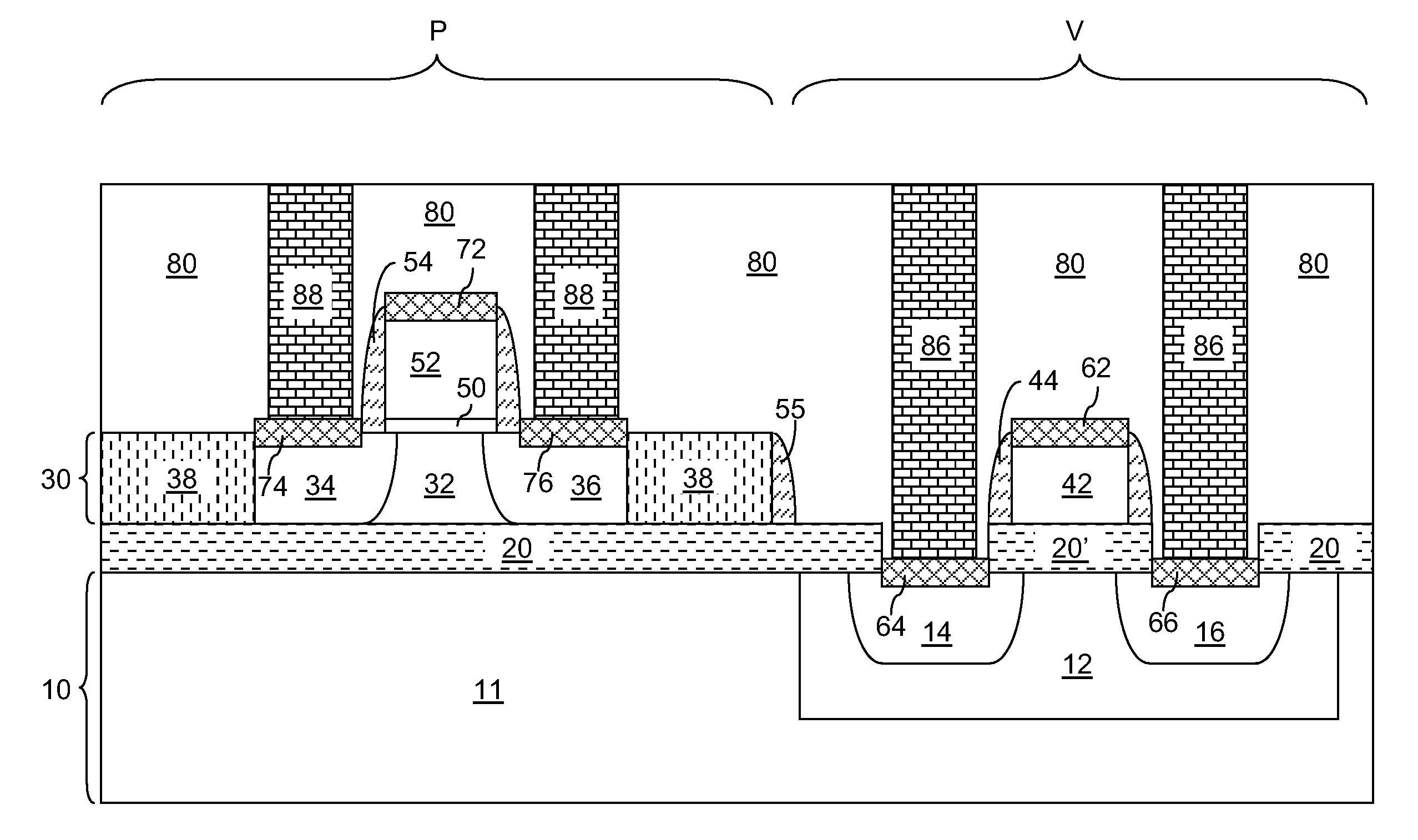
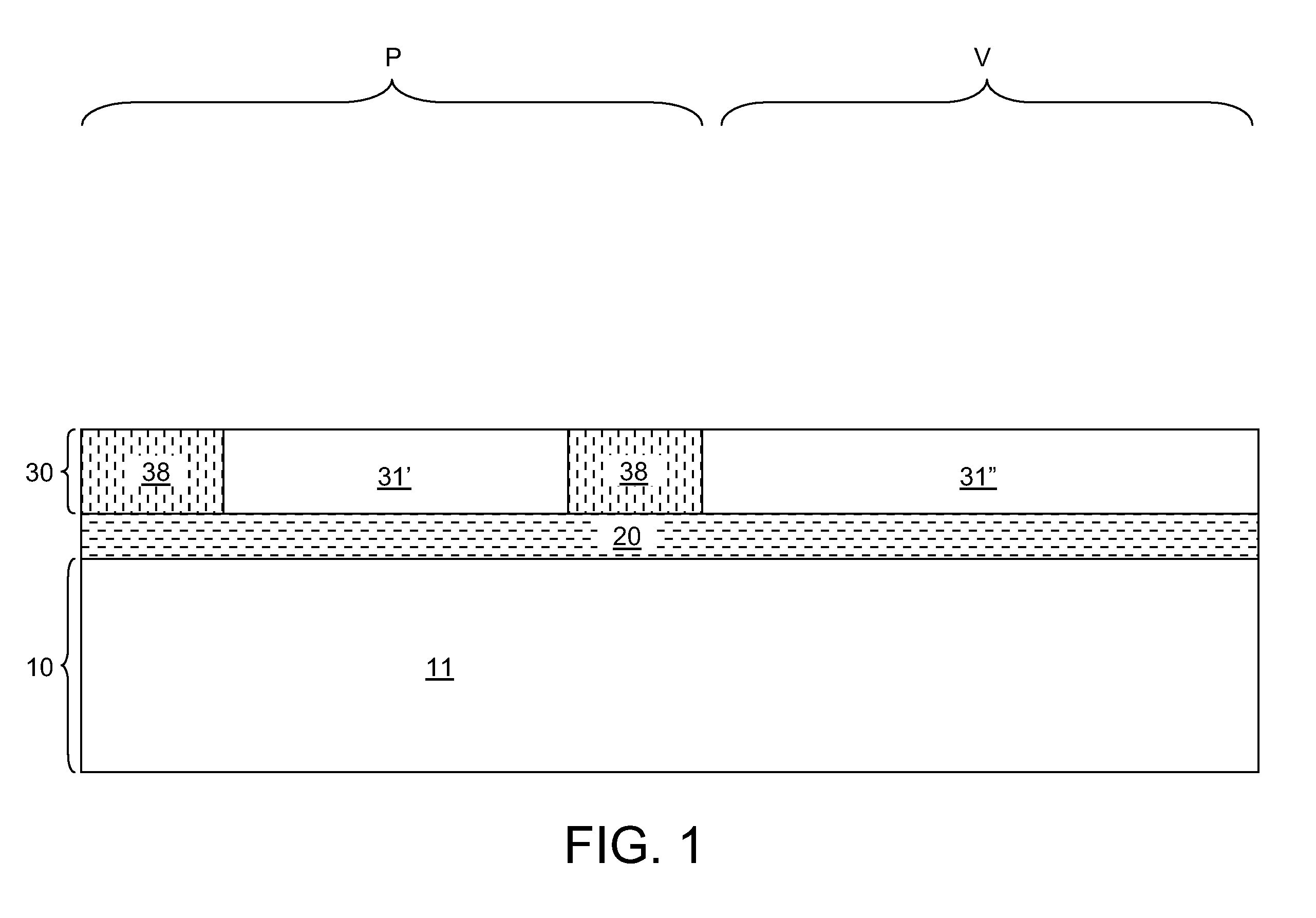
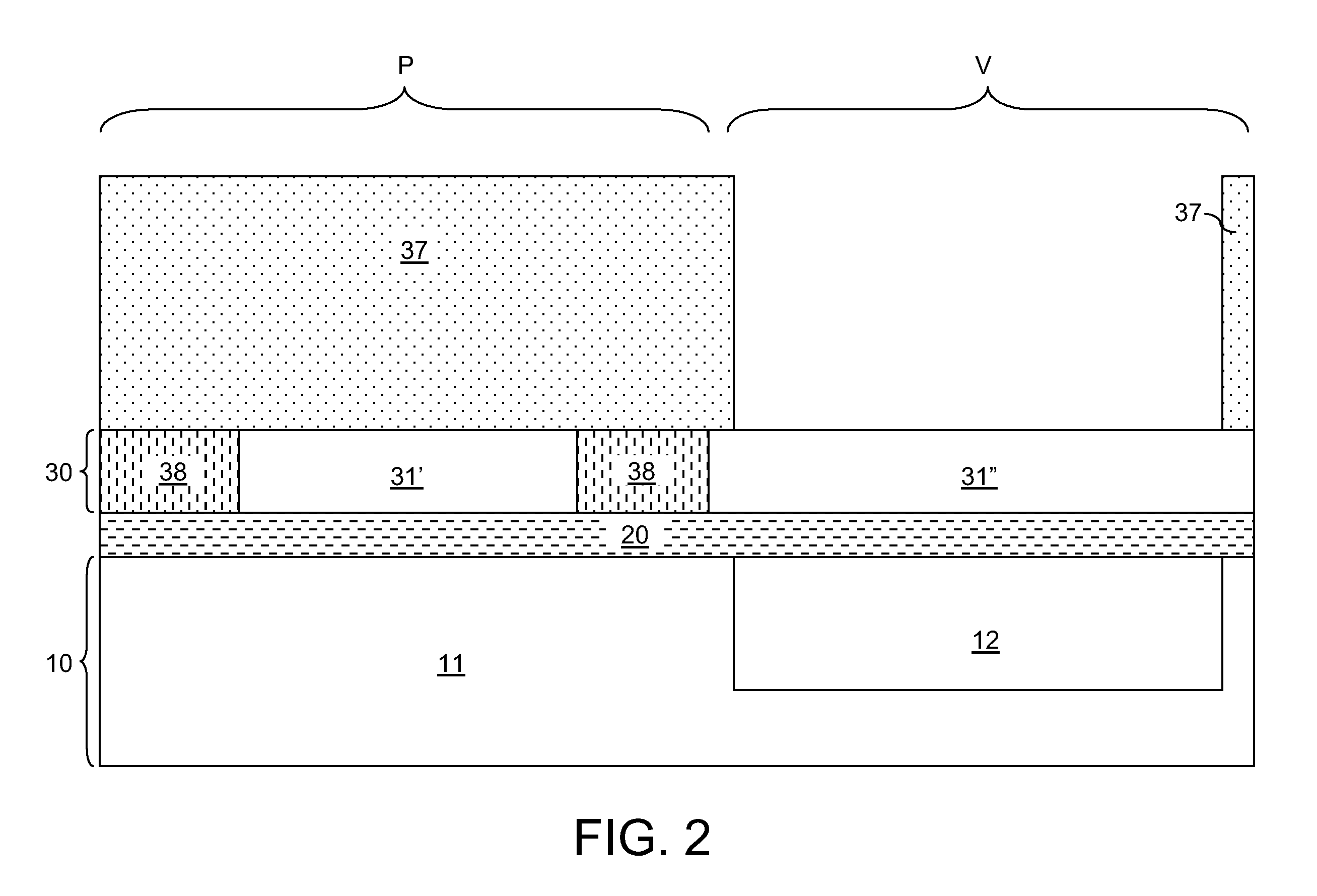
[0038]Referring to FIG. 1, a first exemplary semiconductor structure according to the present invention comprises a semiconductor substrate including a stack, from bottom to top, of a bottom semiconductor layer 10, a buried insulator layer 20, and a top semiconductor layer 30. The area of the semiconductor substrate (10, 20, 30) is divided into a high performance device region P and a high voltage device region V, each of which is a complement of the other. The top semiconductor layer 30 includes a first prototype top semiconductor portion 31′ in the high performance device region P and a second prototype top semiconductor portion 31″ in the high voltage device region V. A shallow trench isolation structure 38 comprising a dielectric material laterally abuts and surrounds the first prototype top semiconductor portion 31′ in the high performance device region P.
[0039]At this step, the entirety of the bottom semiconductor layer 10 comprises a first bottom semiconductor portion 11, whi...
second embodiment
[0074]Referring to FIG. 13, a second exemplary semiconductor structure according to the present invention is derived from the first exemplary semiconductor structure of FIG. 13 by removing the second block level photoresist 47 and applying and lithographically patterning a third block level photoresist 49. The third block level photoresist 49 is patterned to cover the entirety of the high performance device region P, while exposing the entirety of the high voltage device region V. The edge of the third block level photoresist 49 after lithographic patterning may, or may not coincide with an edge of the shallow trench isolation structure 38. Employing the third block level photoresist 49 as an etch mask, the exposed semiconductor material in the high voltage device region V, i.e., the entirety of the second prototype top semiconductor portion (See FIG. 3) is removed by an etch, which may be an anisotropic etch, such as a reactive ion etch or chemical downstream etch, or an isotropic ...
PUM
 Abstract
Description
Claims
Application Information


