Rectifier With PN Clamp Regions Under Trenches

Active Publication Date: 2010-02-11
SEMICON COMPONENTS IND LLC
View PDF4 Cites 38 Cited by
  • Summary
  • Abstract
  • Description
  • Claims
  • Application Information

AI Technical Summary

Benefits of technology

[0008]In another embodiment, the semiconductor region includes an epitaxial layer extending over a substrate, and the substrate has a higher doping concentration than the epitaxial layer.

Problems solved by technology

There is a tradeoff, however, between forward voltage drop and reverse leakage current.
Thermal cycles from subsequent processing steps, however, can cause excessive lateral diffusion of the implanted dopants thus limiting cell pitch.

Method used


Image

  • Rectifier With PN Clamp Regions Under Trenches
  • Rectifier With PN Clamp Regions Under Trenches
  • Rectifier With PN Clamp Regions Under Trenches

Examples


Embodiment Construction

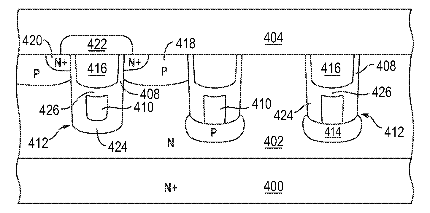
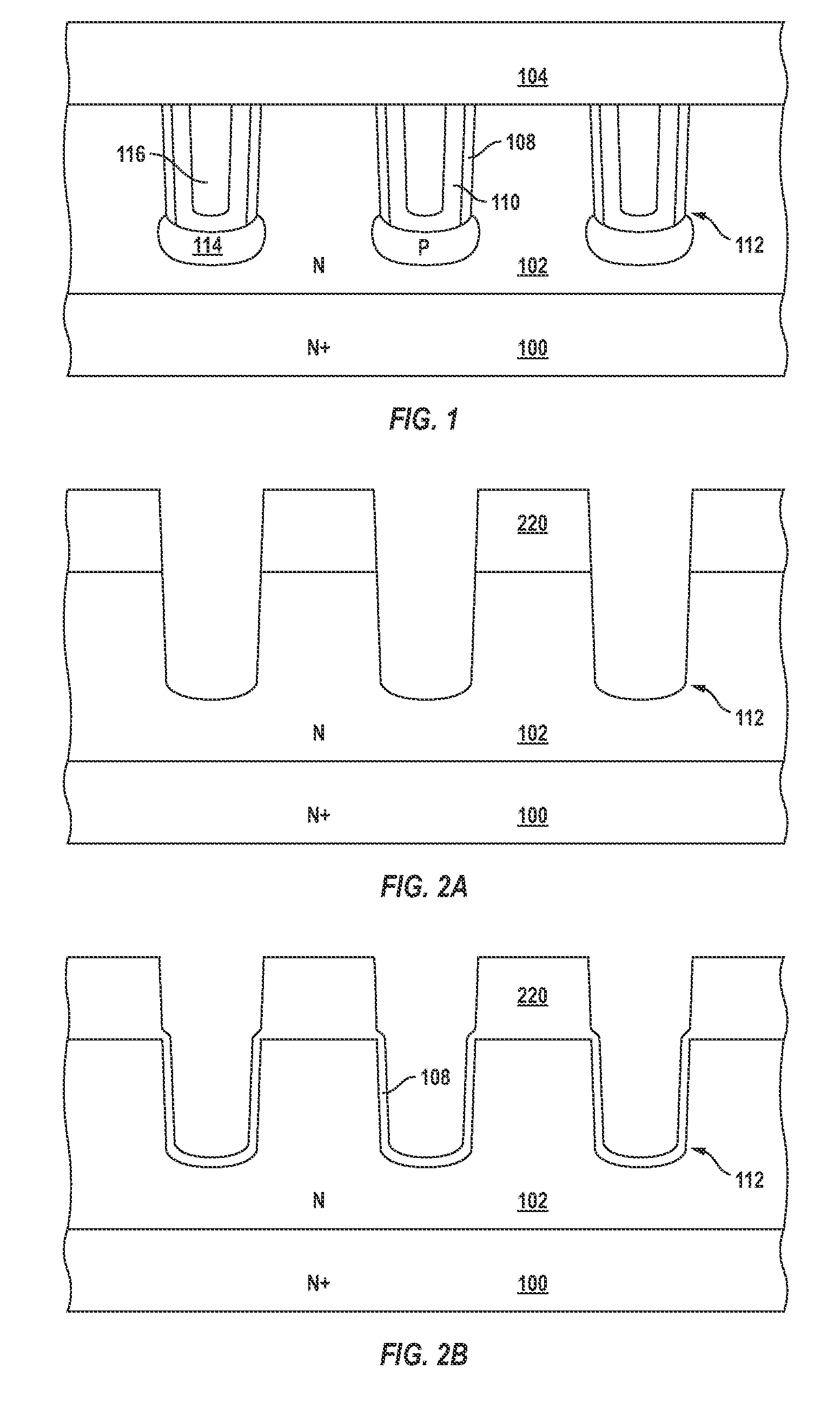
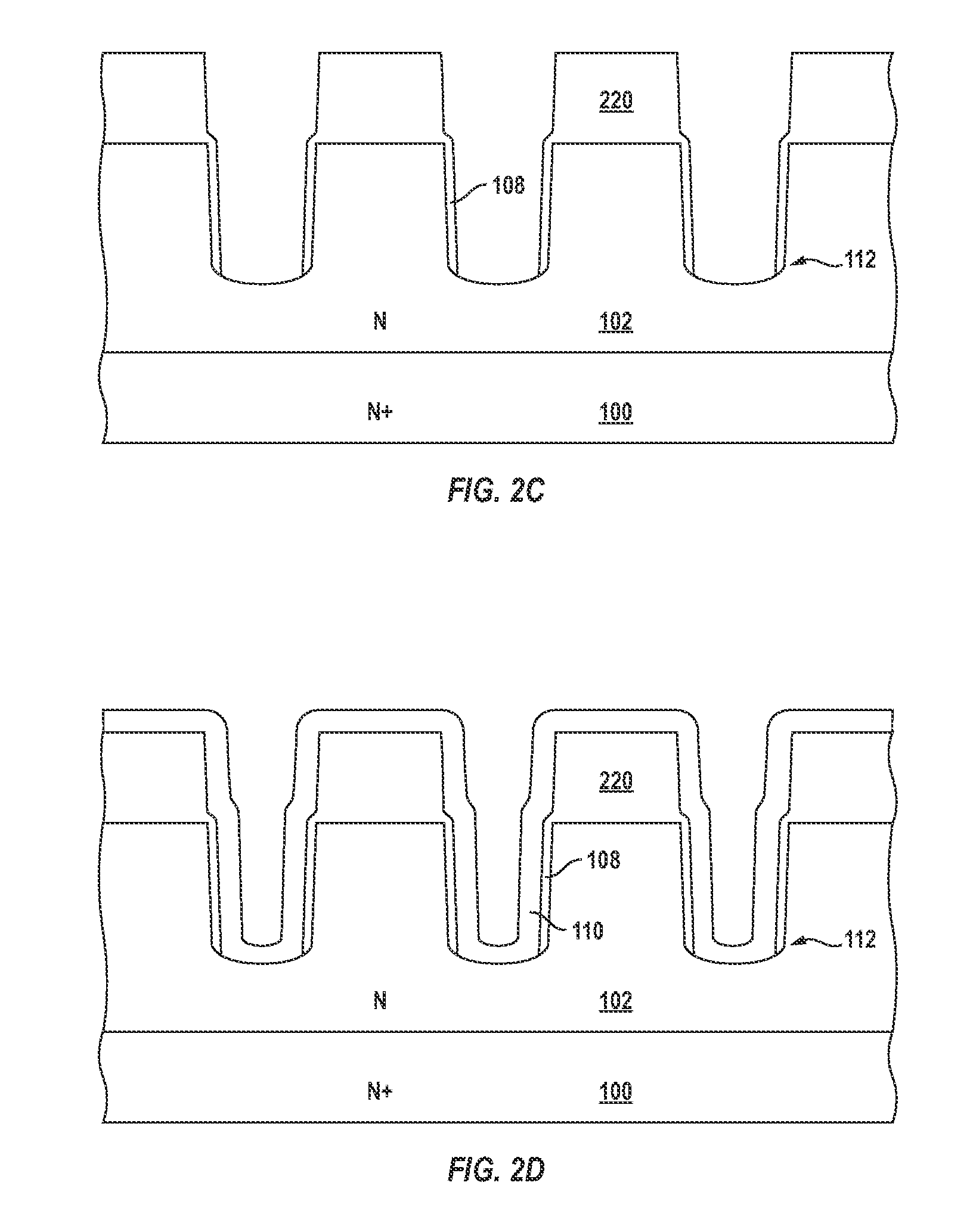
[0020]Embodiments of a TMBS rectifier structure with PN junction clamps and methods of forming the same are described in accordance with the invention. A doped liner is used as the dopant source for the formation of a silicon region below each trench. Whether the liner is doped in-situ or by implant, dopants can be diffused from the doped liner into the surrounding semiconductor region with limited lateral diffusion thus allowing a narrow cell pitch. The silicon region below each trench is of an opposite conductivity type than the surrounding semiconductor region and thus forms a PN junction with the semiconductor region. The PN junction can prevent breakdown from occurring at the Schottky rectifying contact by clamping the reverse voltage at a lower avalanche breakdown of the PN junction. Also, the PN junction is in electrical contact with a conductive material (e.g., the liner) in the trench, and the avalanche current thus flows through the trench rather than through the Schottky ...


PUM


Abstract

A structure that includes a rectifier is formed as follows. A trench is formed in a semiconductor region of a first conductivity type. A dielectric layer is formed along opposing sidewalls of the trench but is discontinuous along the bottom of the trench. A doped liner is formed over the dielectric layer and along the bottom of the trench. The doped liner includes dopants of a second conductivity type and is in direct contact with the semiconductor region along the bottom of the trench. A portion of the dopants are diffused from the doped liner into the semiconductor region along the bottom of the trench to form a doped region. The doped region forms a PN junction with the surrounding semiconductor region.

Description

BACKGROUND OF THE INVENTION[0001]The present invention relates in general to semiconductor technology and in particular to structures and methods for forming performance enhancing PN clamps in such semiconductor structures as trench MOS barrier Schottky (TMBS) rectifiers.[0002]Semiconductor-based power rectifiers are well known and have been used in power electronic systems for many decades. Schottky rectifiers have generally been used in applications operating at mid to low voltages due to their low on-state voltage drop and fast switching speed. Schottky rectifiers can be optimized by changing the Schottky contact metal to alter the barrier height. There is a tradeoff, however, between forward voltage drop and reverse leakage current. As the barrier height is reduced, the forward voltage drop decreases but the reverse leakage current increases. On the other hand, as the barrier height is increased, the forward voltage drop increases but the reverse leakage current decreases.[0003]...

Claims


Application Information

Patent Timeline
IPC IPC(8): H01L29/872
CPCH01L27/0727H01L29/0623H01L29/0626H01L29/1608H01L29/20H01L29/2003H01L29/8725H01L29/66143H01L29/7806H01L29/7808H01L29/7813H01L29/872H01L29/407
Inventor RINEHIMER, MARK
Owner SEMICON COMPONENTS IND LLC
Why Eureka
Try Eureka