Package structure

a technology of packaging structure and semiconductor, applied in the direction of semiconductor/solid-state device details, semiconductor devices, printed circuits, etc., can solve the problems of affecting the quality of the product, so as to improve the wiring layout density, enhance the electrical performance, and enhance the electrical quality

Active Publication Date: 2010-02-11
UNIMICRON TECH CORP
View PDF0 Cites 36 Cited by
  • Summary
  • Abstract
  • Description
  • Claims
  • Application Information

AI Technical Summary

Benefits of technology

[0014]In summary, the purpose of the package structure disclosed in the present invention is to electrically connect the first electrode pads to the second electrode pads by means of through-silicon vias. As a result, in contrast to prior arts, the semiconductor chip of the present invention is electrically connected to the two

Problems solved by technology

However, the conventional BGA semiconductor package structure usually fails to enhance electrical properties and electrical performance during high-fre

Method used


Image

  • Package structure
  • Package structure
  • Package structure

Examples


Embodiment Construction

[0018]The following embodiments are provided to illustrate the disclosure of the present invention, these and other advantages and effects can be apparent to those ordinarily skilled in the art after reading the disclosure of this specification.

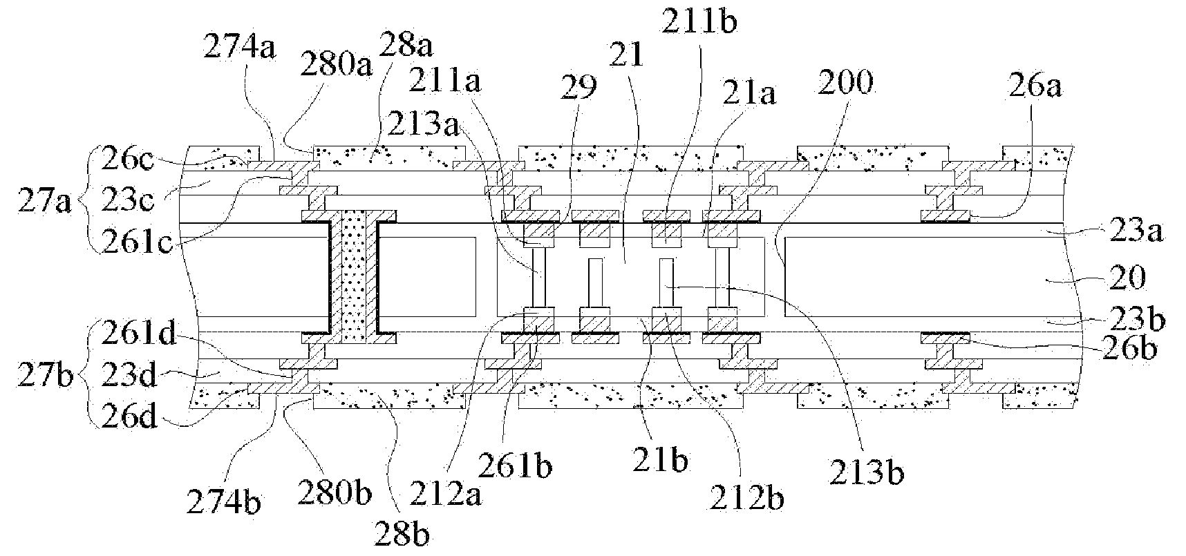
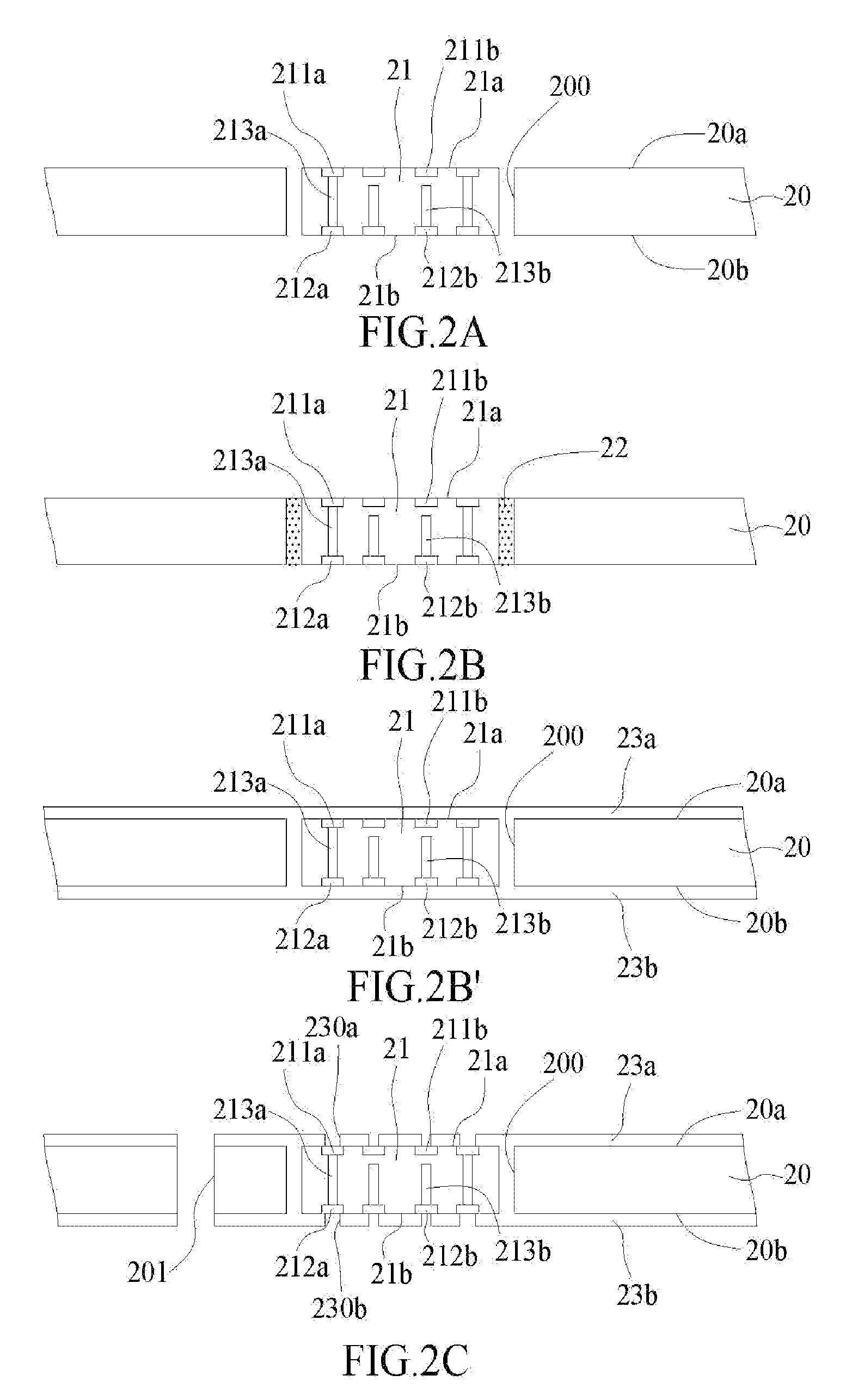
[0019]FIGS. 2A to 2G are cross-sectional diagrams showing a package structure according to an embodiment of the present invention. As shown in 2A, a core board 20 is provided, which may be a wireless substrate, a semi-finished resin layer, a circuit board having circuit traces, or an insulating board, wherein the semi-finished resin layer refers to a resin layer that has not been fully baked. The core board 20 comprises a first surface 20a, an opposite second surface 20b, and at least a through cavity 200 penetrating the first surface 20a and second surface20b and receiving a semiconductor chip 21.

[0020]The semiconductor chip 21 has an active surface 21a and an opposite inactive surface 21b. The active surface 21a and the inactive surface 21b...


PUM


Abstract

Disclosed is a package structure including a semiconductor chip disposed in a core board having a first surface and an opposite second surface. The package structure further includes a plurality of first and second electrode pads disposed on an active surface and an opposite inactive surface of the semiconductor chip respectively, the semiconductor chip having a plurality of through-silicon vias for electrically connecting the first and second electrode pads. As a result, the semiconductor chip is electrically connected to the two sides of the package structure via the through-silicon vias instead of conductive through holes, so as to enhance electrical quality and prevent the inactive surface of the semiconductor chip from occupying wiring layout space of the second surface of the core board to thereby increase wiring layout density and enhance electrical performance.

Description

FIELD OF THE INVENTION[0001]The present invention relates to package structures, and more particularly, to a package structure with an embedded semiconductor chip.DESCRIPTION OF RELATED ART[0002]As the size of electronics products is trending small, the dimensions of the packaging substrates for carrying semiconductor chips or electronics components are decreasing. There are a variety of semiconductor packages. Ball Grid Array (BGA), for example, is an advanced semiconductor package that allows more I / O connections per unit area of the packaging substrate so as to meet the requirement for high integration of semiconductor chips.[0003]A conventional BGA semiconductor package structure is formed by adhering the inactive surface of the semiconductor chip to the packaging substrate for wire bonding or, alternatively, by flip-chip connecting the active surface of the semiconductor chip to the packaging substrate and then implanting solder balls to the back of the packaging substrate for ...

Claims


Application Information

Patent Timeline
IPC IPC(8): H01L23/538
CPCH01L23/5383H01L2224/2518H01L23/5389H01L24/19H01L24/20H01L2224/04105H01L2224/20H01L2924/01029H05K1/185H05K3/4608H01L2924/01024H01L2924/01033H01L2924/014H01L24/25H01L2224/221H01L23/5384
Inventor HSU, SHIH PING
Owner UNIMICRON TECH CORP
Why Eureka
Try Eureka