Light-emitting device having injection-lockable semiconductor ring laser monolithically integrated with master laser

a semiconductor ring laser and monolithic integration technology, applied in semiconductor lasers, laser optical resonator construction, laser details, etc., can solve the problems of poor sensitivity of linbosub>3/sub>modulators, unattractive high half, etc., and achieve the effect of convenient use in practi

Active Publication Date: 2010-02-11
STC UNM
View PDF6 Cites 21 Cited by
  • Summary
  • Abstract
  • Description
  • Claims
  • Application Information

AI Technical Summary

Benefits of technology

[0013]The present invention provides a semiconductor light-emitting device comprising a semiconductor ring laser (SRL) section monolithically integrated on a substrate with a distributed feedback (DFB) master laser section or distributed Bragg reflector (DBR) master laser section such that the ring laser section can be operated in an injection locking mode while being subjected to direct injection current modulation. The monolithic device may be microchip-size that yields a low-cost ultrafast (over 100 GHz bandwidth) functional optical light transmitter that will be easy to use in practice.
[0014]In an illustrative embodiment of the present invention, the device incorporates a SRL, DBR or DFB laser, waveguides, directional couplers, detector and nonreciprocating waveguide elements monolithically integrated on a semiconducting substrate. All the functional elements or sections of the device have single-transverse-mode ridge waveguide structure that may be identical for some or all of them, and share one or more layers of the semiconductor wafer structure spanning the entire length of the chip. The monolithically integrated ring laser section and DBR or DFB master laser section have identical or nearly identical single-transverse-mode ridge-waveguide laser structure and share a system of layers comprising the active region of both. A waveguide section with the same waveguide structure and system of layers is provided between and shared by the master laser section and the ring laser section, and used to transmit the output from the master DBR or DFB laser and inject it into the SRL. Non-reciprocating curved waveguide sections are provided branching off from that “injecting” waveguide to suppress any optical feedback from the SRL to the master DBR or DFB laser. The ring laser section may include an S-shaped waveguide section to promote a unidirectional operation of the ring laser. A waveguide directional coupler section is provided proximate the ring laser section to collect its output. An integrated photodetector located at the backside of the master DBR or DFB laser is provided to monitor the emission from the master laser. The device includes independent electrical contacts to apply direct injection current to the master laser section and the S-shaped waveguide section, to apply direct injection current and high-speed modulated current signal to the ring laser section, and to apply a reverse bias voltage to the photodetector in a manner to provide injection locking of the directly modulated ring laser. Optional electrical contacts can be supplied for the passive waveguide sections to reduce optical loss and provide controllable amplification of the circulating optical signal.
[0015]The present invention also envisions a method of injection locking a directly modulated semiconductor ring laser to achieve enhanced modulation bandwidth by integrating a semiconductor ring laser section with a semiconductor master laser section on a semiconducting substrate so that the former receives light emitted from the master laser section and by selective tuning different input currents in a manner to establish an injection locking mode of operation of the ring laser section and to adjust the resonant frequency offset between the master laser section and the semiconductor ring laser section such as to improve modulation bandwidth of the ring laser.
[0017]Practice of the present invention can be advantageous to provide high performance, small size, low cost, ultra-high-speed integrated light-emitting devices for all levels of telecommunication networks. Development of inexpensive ultrafast chips operating at speeds close to or exceeding 100 GHz bandwidth will have a huge societal impact by increasing the transmission capacity of fiber-based networks.

Problems solved by technology

The drawback of the Ti:LiNbO3 modulators, however, is their poor sensitivity, as represented by their unattractively high half-wave voltage Vπ.
Very high modulation frequency and broad-band performance of the Ti:LiNbO3 modulators come at the expense of too high Vπ, which makes them less attractive for system applications [Cox 2006].
However, the technology of polymer modulators is still very immature, with most of the development effort being focused on the polymer material itself.
In general, the polymers with larger EO effect are the least stable against temperature and optical power, which casts doubt on long-term stability of polymer materials [Cox 2006].
In addition, the frequency response of any EO modulator is typically determined by the electrode RF propagation loss and the phase mismatch between the optical beam and modulation microwave [Chung 1991], [Gopalakrishnan 1994], [Chang 2002], which makes overall design and fabrication of these devices complex and costly.
However, their frequency response has limited the commercial use of directly-modulated lasers to digital transmission not exceeding 10 Gb / s.
Both approaches, however, involve higher injection current densities, which could result in optical damage to the laser facets and excessive heating.
Safe levels of injection current therefore limit the modulation bandwidth in semiconductor lasers.
Thus, under modulation conditions, the slave laser output may exhibit a damped oscillation at the beat frequency ωinj−ωshift due to interference between those two fields.
A large relaxation oscillation damping rate γRO can undermine the ability of the laser to respond to fast modulation.
In practice, directly modulated lasers often suffer from high distortions near the resonance frequency fRO, which makes them useful only at RF frequencies much lower than fRO [Lau 1984].
Another factor limiting modulation bandwidth in injection-locked lasers, evident in all strong-injection-locking experiments, is a sharp roll-off of their modulation response that occurs at low modulation frequencies, before the modulation response gets enhanced by the resonance frequency.
(3)-(5), hence they would be ineffective in increasing ωp.
The inherent design trade-off between these parameters, however, makes further optimization of both edge-emitting lasers and VCSELs for enhanced high-speed performance very problematic.
While injection-locked VCSELs benefit greatly from very short cavities and, hence, very small τrt, their high-speed performance, at the same time, is compromised by very high mirror reflectivity of a typical VCSEL, resulting in coupling rate coefficients similar to edge emitters.
This, however, can hardly be realized with VCSELs, notable for their very high mirror reflectivity.
In addition, stand-alone VCSELs pose a very serious alignment problem in injection-locking experiments and, at the same time, are not suitable for monolithic integration when injection locking is the requirement.
We believe VCSELs are very hard to be optimized for any further improvement in their speed.

Method used


Image

  • Light-emitting device having injection-lockable semiconductor ring laser monolithically integrated with master laser
  • Light-emitting device having injection-lockable semiconductor ring laser monolithically integrated with master laser
  • Light-emitting device having injection-lockable semiconductor ring laser monolithically integrated with master laser

Examples


Embodiment Construction

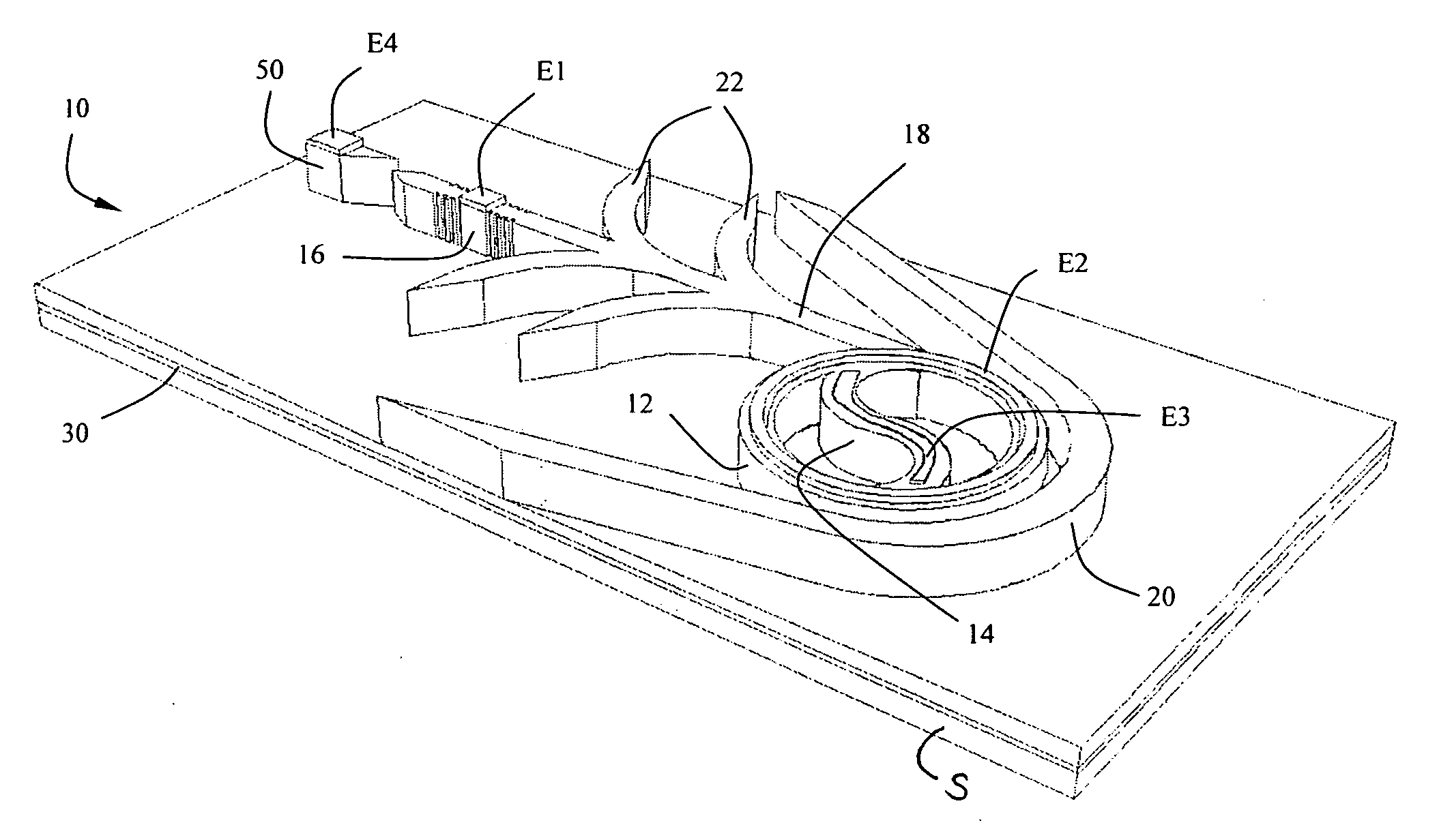
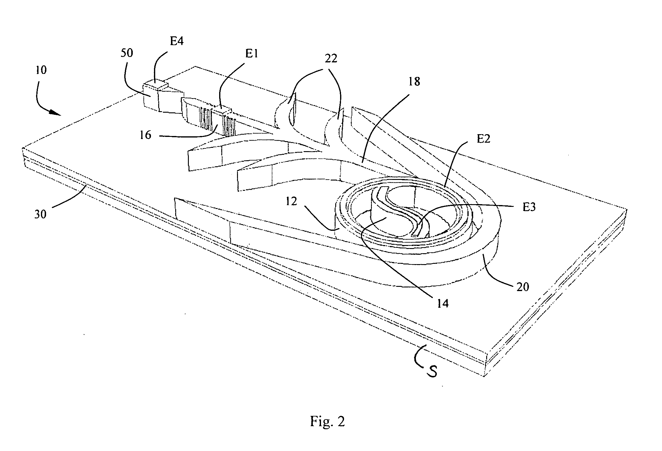
[0024]As shown in FIG. 2, an embodiment of the present invention provides a semiconductor light-emitting device 10 having a unidirectional semiconductor ring laser (USRL) section 12 monolithically integrated with a high-power semiconductor distributed Bragg reflector (DBR) (alternatively, distributed feedback, DFB) laser section 16 in a manner that can provide an injection locking mode of operation of the USRL section (slave laser) by injecting light from the DBR (DFB) laser section (master laser) wherein the slave laser section is substantially locked to the same frequency as the master laser section and wherein a significant increase in modulation bandwidth is thereby provided. The above integration thus can result in a low-cost, ultrafast (over 100 GHz) functional optical light-emitting transmitter.

[0025]Use of a unidirectional semiconductor ring laser (USRL) section as a slave laser in practice of the invention is advantageous to provide minimal back reflections (eliminating the...


PUM


Abstract

A semiconductor ring laser (SRL) section is monolithically integrated with a DFB or DBR master laser section on a semiconductor substrate of a light-emitting device to provide an injection locking mode of operation that can result in low-cost ultrafast (over 100 GHz) functional chip that will be easy to use in practice.

Description

RELATED APPLICATION[0001]This is a continuation-in-part application of Ser. No. 12 / 387,714 filed May 6, 2009, which claims benefits of provisional application Ser. No. 61 / 126,918 filed May 7, 2008, the disclosures of both of which are incorporated herein by reference.FIELD OF THE INVENTION[0002]The present invention relates to semiconductor light-emitting laser devices and, in particular, to an injection-lockable semiconductor ring laser monolithically integrated with a DBR or DFB semiconductor laser to improve ultrahigh frequency performance of semiconductor light-emitting laser devices for both digital and analog applications.BACKGROUND OF THE INVENTION[0003]A. Direct Modulation vs. External Modulation of Semiconductor Laser Output[0004]The continuing increase of transmission rates at all levels of telecommunication networks and fiber-based RF photonic systems raises demand for very high-speed, low cost optical transmitters. Much effort has been put into developing wide-bandwidth ...

Claims


Application Information

Patent Timeline
Patent Type & Authority Applications(United States)
IPC IPC(8): H01S5/026H01S3/098H01S5/12
CPCH01S5/026H01S5/0264H01S5/1003H01S5/1032H01S5/50H01S5/12H01S5/125H01S5/2275H01S5/4006H01S5/1071H01S5/1237
Inventor OSINSKI, MAREK A.QASSIM, OMAR K.WITHERS, NATHAN J.SMOLYAKOV, GENNADY A.
Owner STC UNM
Why Eureka
Try Eureka