

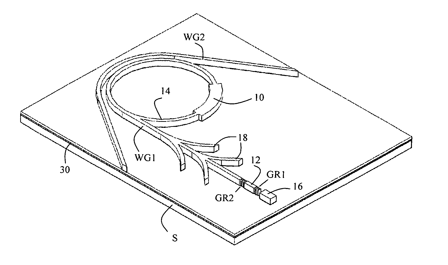
Light-emitting device having photon-lifetime modulation
a light-emitting device and photon-lifetime technology, applied in the field of laser systems, can solve the problems of poor sensitivity of linbosub>3/sub>modulators, unattractive half, etc., and achieve the effect of convenient use in practi
- Summary
- Abstract
- Description
- Claims
- Application Information
AI Technical Summary
Benefits of technology
Problems solved by technology
Method used
Image

Examples
Embodiment Construction
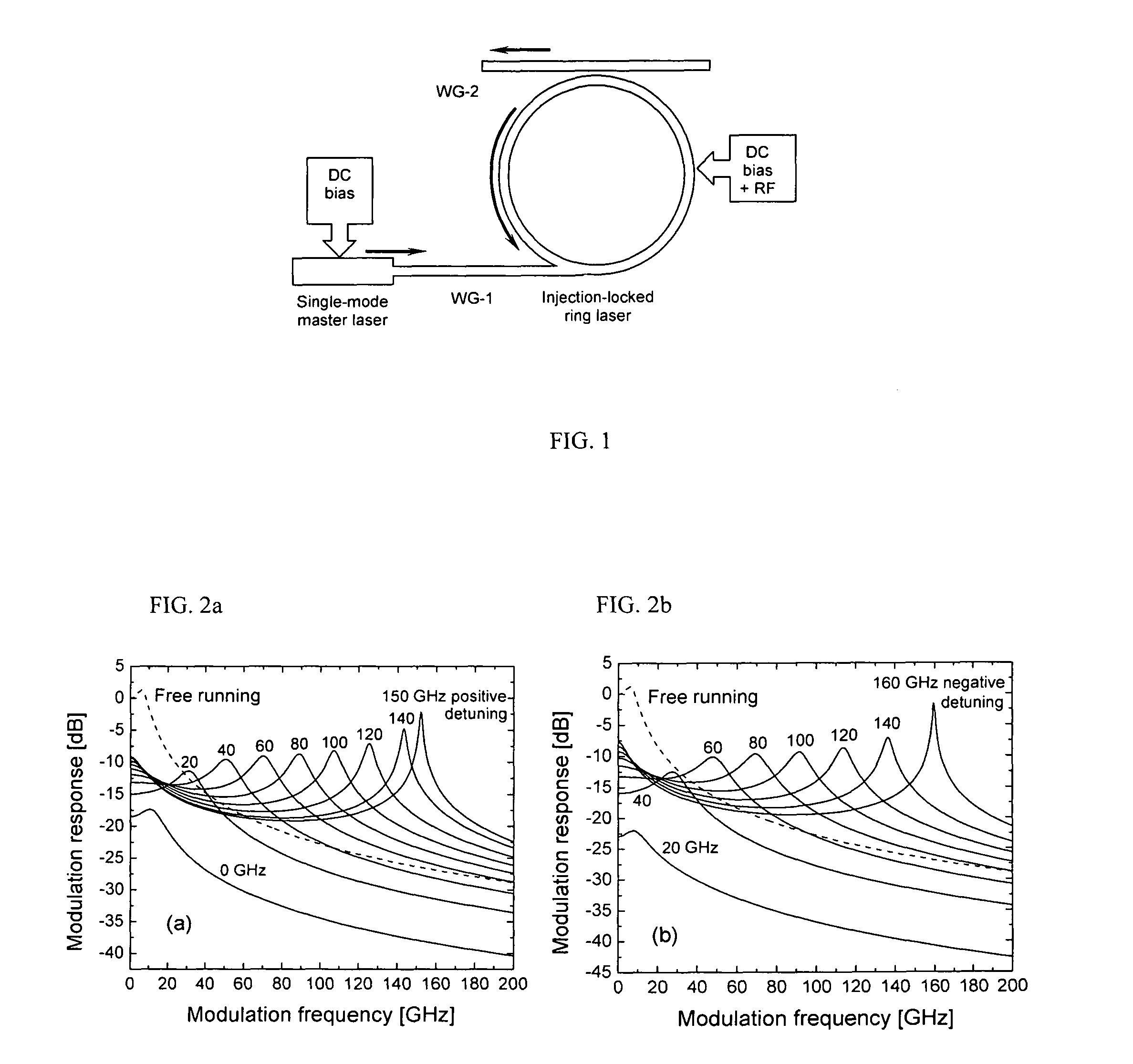
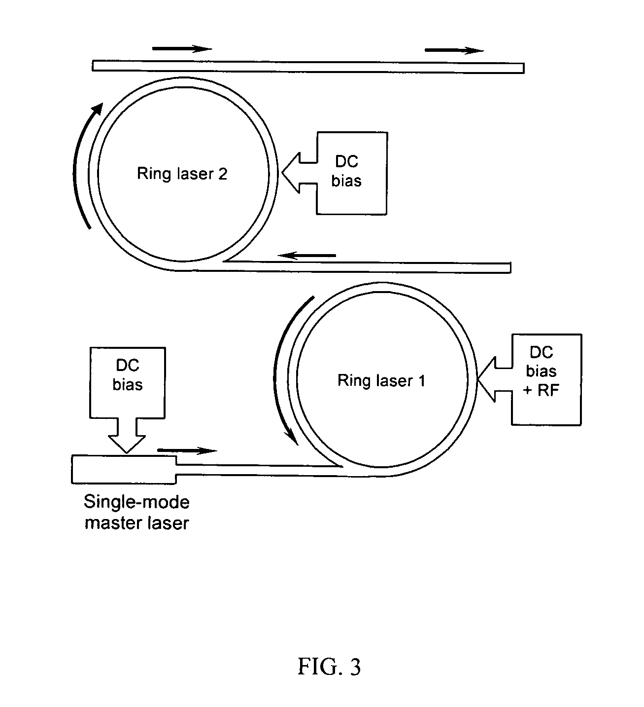
[0044]The following description is offered to further illustrate the invention without limiting it. Optical injection locking has been actively researched for its potential to improve ultrahigh-frequency performance of semiconductor lasers for both digital and analog applications as described in U.S. Pat. No. 8,009,712, the disclosure of which is incorporated herein by reference. The highest experimentally observed 3-dB modulation bandwidth of ˜80 GHz, by far exceeding those achieved for free-running devices, has been reported in injection-locked vertical-cavity surface-emitting lasers (VCSELs). While laboratory experiments with injection-locked VCSELs demonstrated record-high values for enhanced modulation bandwidth, they require multiple hybrid components that need to be carefully aligned. Their vertical geometry makes VCSELs unsuitable for monolithic integration with the DBR lasers used as masters. Aside from that, typical for all optical-injection-locking schemes, the modulation...
PUM
 Abstract
Description
Claims
Application Information