Thin body silicon-on-insulator transistor with borderless self-aligned contacts

a silicon-on-insulator transistor and self-aligning technology, applied in the field of thin body field-effect transistors with electrical contacts, can solve the problems of inoperable devices, considerable challenge in electrical contact formation,

Inactive Publication Date: 2010-02-18
GLOBALFOUNDRIES INC
View PDF18 Cites 28 Cited by
  • Summary
  • Abstract
  • Description
  • Claims
  • Application Information

AI Technical Summary

Benefits of technology

[0004]Briefly, in accordance with the present invention, disclosed in one embodiment is a method for fabricating a thin-silicon-on-insulator transistor with borderless self-aligned contacts is disclosed. The method includes forming a gate stack on a silicon layer that is above a buried oxide layer. The gate stack includes a gate oxide layer on the silicon layer and a gate electrode laye

Problems solved by technology

The formation of electrical contacts to electronic and memory devices is a considerable challenge as the integration density of these devices is increased as a consequence of technology scaling.
Defi

Method used


Image

  • Thin body silicon-on-insulator transistor with borderless self-aligned contacts
  • Thin body silicon-on-insulator transistor with borderless self-aligned contacts
  • Thin body silicon-on-insulator transistor with borderless self-aligned contacts

Examples


Embodiment Construction

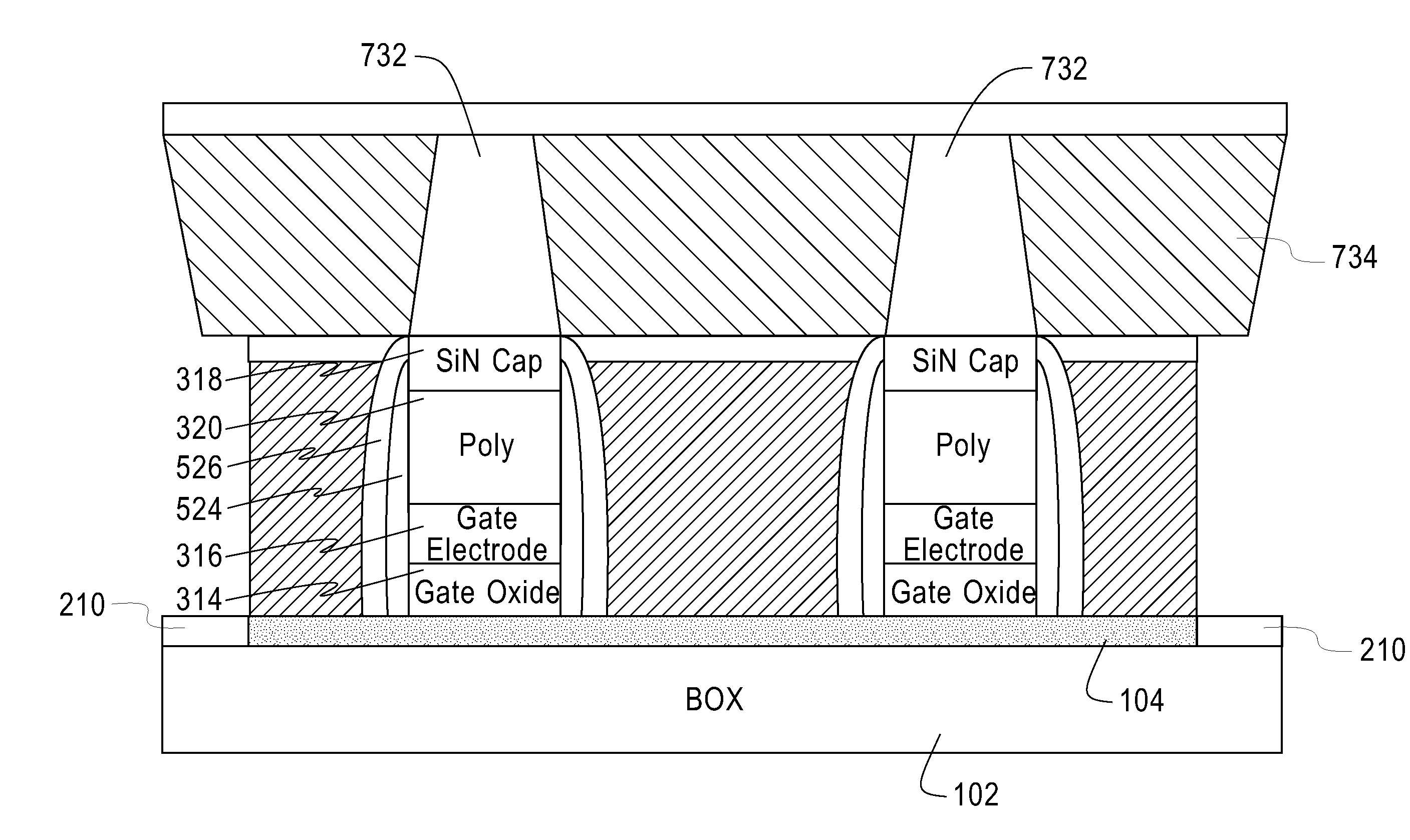
[0008]Embodiments of the present invention provide thin silicon-on-insulator field-effect transistors with borderless self-aligned electrical contacts. Contacts that are self aligned to the source and drain are highly desirable to overcome the misalignment problem discussed above. Generally, an epitaxial layer of Si is grown in the source and drain region of thin body devices, often referred to as a raised source drain (“RSD”). The RSD lowers the external resistance of the device by mitigating the so called “current crowding” effect. It simultaneously provides the requisite volume of Si to form a silicide without fully siliciding the source and drain. The RSD causes an increased capacitance from the source and drain to the gate. This capacitance is present regardless of the gate height.

[0009]However, various embodiments of the present invention provide an advantageous method for forming self-aligned borderless contacts to thin body FET devices. These contacts are formed by the epita...


PUM


Abstract

A method for fabricating a thin-silicon-on-insulator transistor with borderless self-aligned contacts is disclosed. A gate stack is formed on a silicon layer that is above a buried oxide layer. The gate stack includes a gate oxide layer on the silicon layer and a gate electrode layer on the gate oxide layer. A hard mask on top of the gate stack is formed. An off-set spacer is formed surrounding the gate stack. A raised source/drain region is epitaxially formed adjacent to the off-set spacer. The raised source/drain region is grown slightly about a height of the gate stack including the hard mask. The raised source/drain region forms borderless self-aligned contact.

Description

FIELD OF THE INVENTION[0001]The present invention generally relates to the field of semiconductors, and more particularly relates to thin body field-effect transistors with electrical contacts on semiconductor substrates.BACKGROUND OF THE INVENTION[0002]Complementary Metal Oxide Semiconductor (“CMOS”) Field Effect Transistors (“FETs”) are employed in almost every electronic circuit application, such as signal processing, computing, and wireless communications. One known type of FET is a Silicon-On-Insulator (“SOI”) FET. The formation of electrical contacts to electronic and memory devices is a considerable challenge as the integration density of these devices is increased as a consequence of technology scaling.[0003]For example, the projected contact pitch for 32, 22, and 15 nm nodes are 130, 100, and 80 nm, respectively. In order to fit the contact between adjacent gates, contacts must be made at dimensions approaching the gate length of the device unlike previous technologies wher...

Claims


Application Information

Patent Timeline
IPC IPC(8): H01L29/72H01L21/84
CPCH01L29/6656H01L29/78618H01L29/66772H01L29/66628
Inventor BABICH, KATHERINA E.GUILLORN, MICHAEL A.LAUER, ISAACMAJUMDAR, AMLAN
Owner GLOBALFOUNDRIES INC
Why Eureka
Try Eureka