Resistive random access memory and method for fabricating the same

a random access memory and resistive technology, applied in the field of resistive random access memory elements, can solve the problems of loss of endurance, resistive random access memory b>20/b> does not improve enduran

Active Publication Date: 2010-02-18
TAIWAN SEMICON MFG CO LTD
View PDF12 Cites 108 Cited by
  • Summary
  • Abstract
  • Description
  • Claims
  • Application Information

AI Technical Summary

Problems solved by technology

The conventional resistive random access memory 10, however, exhibits extremely unstable operating voltage (in particular SET voltage) after repeated and continuous conversion of resistance, resulting in loss of endurance.
Even so, the resistive random access memory 20 does not improve upon endurance.

Method used


Image

  • Resistive random access memory and method for fabricating the same
  • Resistive random access memory and method for fabricating the same
  • Resistive random access memory and method for fabricating the same

Examples


example 1

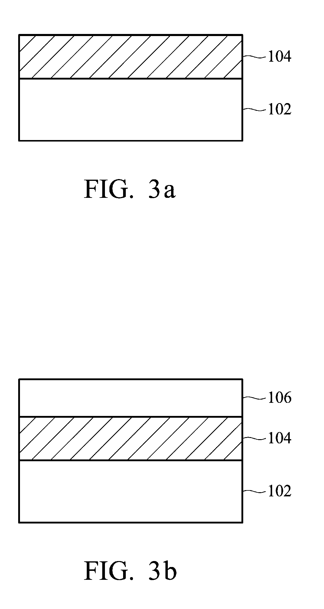
[0034]A silicon substrate was provided. A TiN layer with a thickness of 50 nm serving as bottom electrode was formed on the substrate. Next, an HfO layer with a thickness of 20 nm was formed on the bottom electrode, serving as a metal oxide layer. Next, a Ti layer with a thickness of 10 nm was formed on the HfO layer. Next, a TiN layer with a thickness of 50 nm was formed on the Ti layer. Finally, the above structure was subjected to an annealing treatment, thereby forcing the oxygen atoms of the HfO to migrate into the Ti to form TiO. Thus, obtaining a RRAM element A.

[0035]The content of the oxygen atoms of the aforementioned structure was measured by an Auger Electron Spectroscopy (AES) before and after annealing, and the results are shown in FIG. 7. The content of the oxygen atoms of the HfO layer was reduced and that of the Ti layer was increased after annealing. Further, the content of the oxygen atoms of the TiN layer was almost the same before and after annealing. Therefore, ...

example 2

[0037]A silicon substrate was provided. A TiN layer with a thickness of 50 nm serving as a bottom electrode was formed on the substrate. Next, an HfO layer with a thickness of 20 nm was formed on the bottom electrode, serving as a metal oxide layer. Next, an Al layer with a thickness of 10 nm was formed on the HfO layer. Next, a TiN layer with a thickness of 50 nm was formed on the Al layer. Finally, the above structure was subjected to an annealing treatment, thereby forcing the oxygen atoms of the HfO to migrate into the Al to form the AlO layer. Thus, obtaining a RRAM element B.


PUM

PropertyMeasurementUnit
thicknessaaaaaaaaaa
thicknessaaaaaaaaaa
thicknessaaaaaaaaaa

Abstract

A resistive random access memory and a method for fabricating the same are provided. The method includes providing a bottom electrode formed on a substrate. A metal oxide layer is formed on the bottom electrode. An oxygen atom gettering layer is formed on the metal oxide layer. A top electrode is formed on the oxygen atom gettering layer. The previous mentioned structure is subjected to a thermal treatment, driving the oxygen atoms of the metal oxide layer to migrate into and react with the oxygen atom gettering layer, thus leaving a plurality of oxygen vacancies of the metal oxide layer.

Description

CROSS REFERENCE TO RELATED APPLICATIONS[0001]This application is based upon and claims the benefit of priority from the prior Taiwan Patent Application No. 97130654, filed on Aug. 12, 2008, the entire contents of which are incorporated herein by reference.BACKGROUND OF THE INVENTION[0002]1. Field of the Invention[0003]The invention relates to a memory element, and more particularly to a resistive random access memory element.[0004]2. Description of the Related Art[0005]For IC (integrated circuit) designers, the ideal semiconductor memory includes random accessibility, non-volatile characteristics, increased capacity, increased speed, reduced power consumption, and unlimited reading and writing functions. Resistive random access memory (RRAM) technology has been gradually recognized as having exhibited the aforementioned semiconductor memory advantages.[0006]Please refer to FIG. 1, a conventional single-pole operation resistive random access memory 10 with a single oxide layer is sho...

Claims


Application Information

Patent Timeline
Patent Type & Authority Applications(United States)
IPC IPC(8): H01L29/45H01L21/44
CPCH01L45/08H01L45/1233H01L45/1658H01L45/1641H01L45/1253H01L45/146H10N70/24H10N70/826H10N70/8833H10N70/041H10N70/046H10N70/841
Inventor LEE, HENGYUANCHEN, PANG-HSUWU, TAI-YUANWANG, CHING-CHIUN
Owner TAIWAN SEMICON MFG CO LTD
Why Eureka
Try Eureka