Oxide multilayered gradient film and RRAM component structured thereby
An oxide film, oxide technology, applied in electrical components, layered products, etc., can solve problems such as difficult to meet practical applications, reduce initialization voltage, etc., achieve excellent transition and memory characteristics, high stability and retention, High retention effect
- Summary
- Abstract
- Description
- Claims
- Application Information
AI Technical Summary
Problems solved by technology
Method used
Image
Examples
Embodiment 1
[0025] Embodiment 1. Preparation process of titanium oxide RRAM components
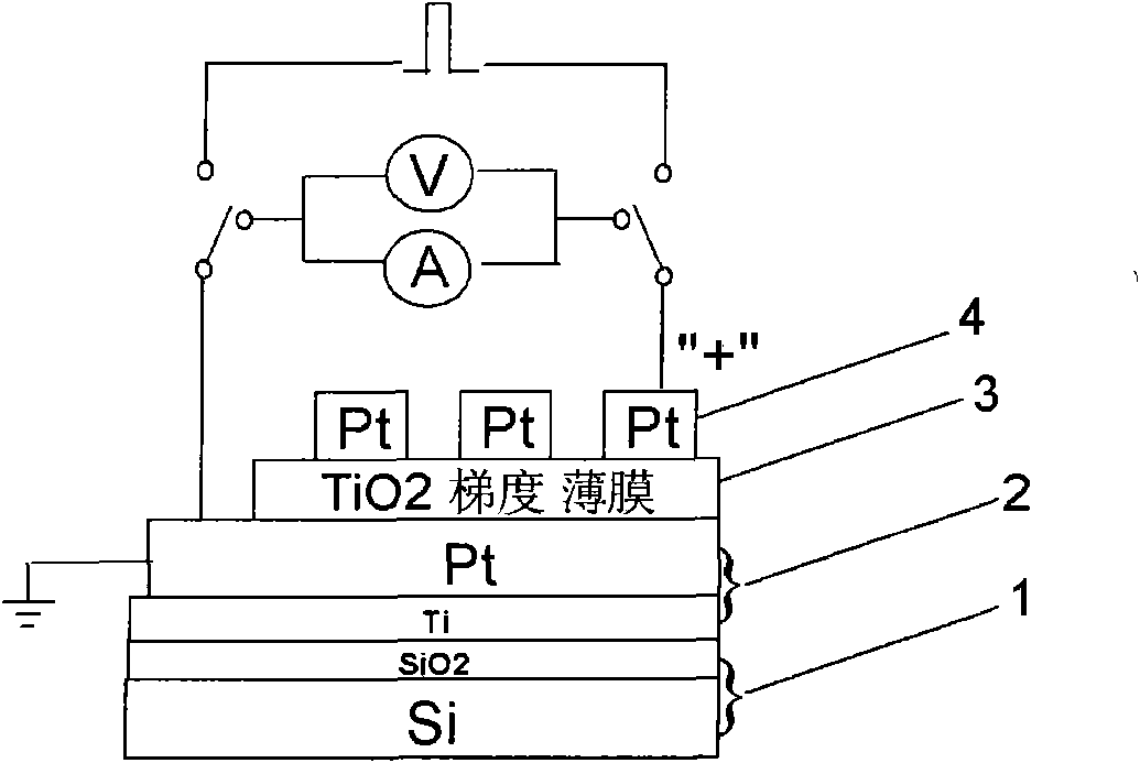
[0026] Choose Pt as the bottom electrode and top electrode layer; choose TiO 2 The gradient film is a resistive oxide layer, and the titanium oxide gradient film RRAM component is prepared, which is characterized in that: a Pt bottom electrode layer 2 is sequentially deposited on the substrate 1, and the middle resistive layer TiO 2 Gradient film 3, Pt top electrode 4. The specific process steps are as follows:
[0027] 1) A Pt bottom electrode 2 is prepared on the Si substrate 1 by a magnetron sputtering process, and the thickness of the Pt electrode is 100-200 nm. Of which SiO 2 It is the natural oxide layer on the surface of single crystal Si, Ti is Pt and SiO 2 The bonding layer between.
[0028] 2) Deposition of TiO by pulsed laser deposition (PLD) 2 Gradient film 3, using TiO 2 Ceramic target, the background vacuum is less than 4×10 -4 Pa, layered deposition of TiO with different oxygen content 2 Grad...
Embodiment 2
[0031] Example 2. N=3 and N=6 TiO 2 Preparation of gradient film
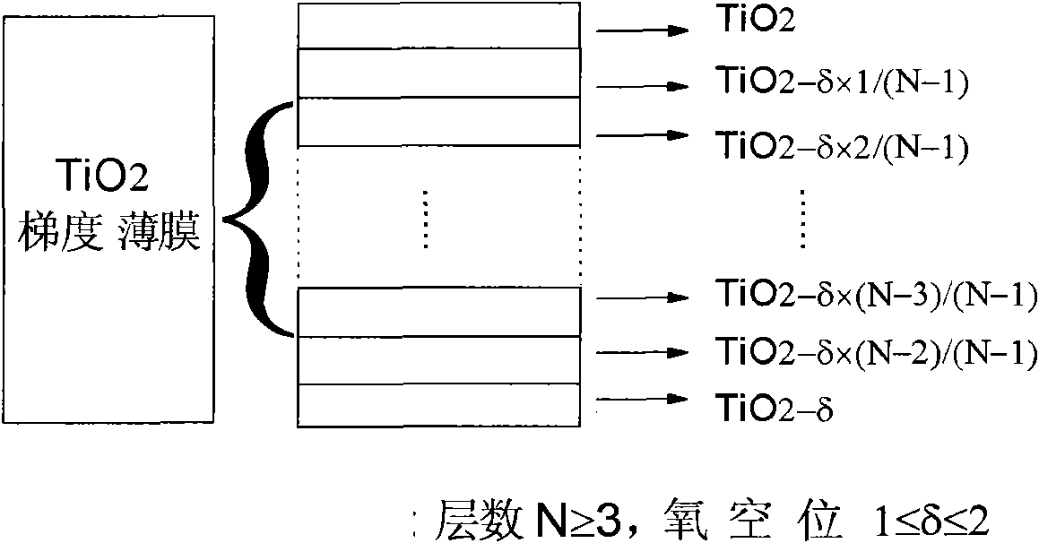
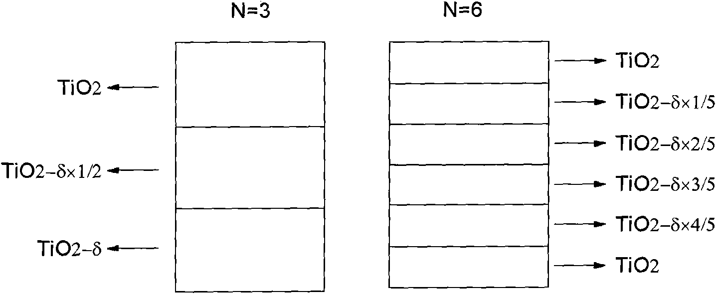
[0032] Theoretically assume TiO 2 The number of layers of the gradient film is N, and the bottom layer near the bottom electrode is TiO 2-δ Thin film, in which the concentration of oxygen vacancies is δ; from bottom to top, the concentration of oxygen vacancies is reduced layer by layer with a step length of δ / (N-1), and after reaching the top layer, it becomes a stoichiometric TiO 2 Film, see attached figure 2 . Attached image 3 Give TiO 2 Two examples of theoretical schematic diagrams of gradient films: the number of layers N=3 and N=6. Theoretically, N can tend to infinity, that is, the gradient film is designed as TiO with continuously changing oxygen vacancies 2 film.
[0033] Use PLD deposition method to deposit TiO 2 Gradient film. In the experiment, first the Pt / Ti / SiO produced in the process step 1) of Example 1 2 The temperature of / Si is controlled within the range of room temperature to 700℃, the pu...
Embodiment 3
[0034] Example 3, N=3 and N=6 TiO 2 Resistance switching properties of gradient films
[0035] N=3 TiO 2 The resistance transition process of gradient film components can be described as: the film is initially in a high resistance state, Image 6 a is the initial I-V curve, and the voltage sweep range is ±1V, showing a significant junction effect: conduction in the positive direction and cut-off in the negative direction, indicating Pt / TiO 2 The Schottky knot on the upper interface plays a major role. Apply negative voltage to a certain value (V forming ~7.4V), the film transforms into a low resistance state, the so-called forming process is like Image 6 Shown in b. Then apply the forward voltage to a certain value (V set ), the film returns to a high resistance state; then a negative voltage is applied to a certain value (V reset ), the film transforms into a low-resistance state, which is a cycle, Image 6 In c is the I-V curve of 2 cycles, which shows that its repeatability ...
PUM
| Property | Measurement | Unit |
|---|---|---|
| Thickness | aaaaa | aaaaa |
Abstract
Description
Claims
Application Information


