
Semiconductor device and method for manufacturing the same

a semiconductor and semiconductor technology, applied in the direction of transistors, electroluminescent light sources, electric lighting sources, etc., can solve the problems of oxide semiconductors affecting the characteristics of transistors as problems, and achieve the effects of stable electrical characteristics, low power consumption, and high reliability

Active Publication Date: 2014-06-05
SEMICON ENERGY LAB CO LTD
View PDF2 Cites 34 Cited by
  • Summary
  • Abstract
  • Description
  • Claims
  • Application Information

AI Technical Summary

Benefits of technology

The patent describes a problem with transistors made using oxide semiconductor for a channel formation region. These transistors can have issues with electrical characteristics due to oxygen vacancies in the oxide semiconductor. The vacancies can lead to the formation of carriers and a reduction in resistance, which negatively impacts the transistor's performance. The objective of the patent is to provide a semiconductor device with a reduced number of oxygen vacancies in the channel formation region of oxide semiconductor, which will have stable electrical characteristics and high reliability. Additionally, the goal is to reduce or suppress the change in gate voltage-drain current characteristics by application of a drain voltage.

Problems solved by technology

In the case where a transistor is formed using an oxide semiconductor for a channel formation region, an oxygen vacancy (also referred to as Vo in this specification) which is formed in the oxide semiconductor affects the transistor characteristics as a problem.

Method used


Image

  • Semiconductor device and method for manufacturing the same
  • Semiconductor device and method for manufacturing the same
  • Semiconductor device and method for manufacturing the same

Examples


example 1

[0487]In this example, measurement results that show how sheet resistance of an oxide semiconductor layer changes before and after heat treatment corresponding to the heat treatment performed after the formation of the oxide insulating film shown in the above embodiment will be described with reference to FIGS. 29, 30, 31, and 32. For example, it can be considered that the oxide semiconductor layer is an i-type in the case where the sheet resistance of the oxide semiconductor layer exceeds the measurement upper limit value of measurement equipment (i.e., exceeds the range) and the oxide semiconductor layer is an n-type in the case where the sheet resistance of the oxide semiconductor layer can be measured.

[0488]As samples for measurements of sheet resistance, the following samples were manufactured: samples which each include an IGZO layer formed over a glass substrate by a sputtering method with a target containing In, Ga, and Zn in an atomic ratio of 1:1:1 (hereinafter the IGZO la...

example 2

[0500]In this example, comparison between an oxide semiconductor layer including an nanocrystal (a nc-OS layer) and a CAAC-OS layer which is made regarding the measurement results that show how sheet resistance of an oxide semiconductor layer changes before and after heat treatment corresponding to the heat treatment performed after the formation of the oxide insulating film shown in the above embodiment will be described with reference to FIGS. 34 and 35.

[0501]As samples for measurements of sheet resistance, the following samples were manufactured: samples which each include an IGZO layer including an nanocrystal formed over a glass substrate by a sputtering method with a target containing In, Ga, and Zn in an atomic ratio of 1:1:1 (hereinafter the IGZO layer is referred to as an nc-OS layer in this example) and samples which each include an IGZO layer including a CAAC-OS layer formed over a glass substrate by a sputtering method (hereinafter the IGZO layer is referred to as a CAAC...

example 3

[0513]In this example, measurement results of diffusion of metal which is used for a conductive layer to an oxide semiconductor layer in the case where heat treatment corresponding to the heat treatment performed after the formation of the oxide insulating film will be described with reference to FIG. 37.

[0514]First, in each measurement sample, an IGZO layer which was an oxide semiconductor layer was formed over a glass substrate by a sputtering method with a target containing In, Ga, and Zn in an atomic ratio of 1:1:1. The IGZO layer was formed under conditions where the flow rates of argon and oxygen were each 100 sccm, the pressure was 0.6 Pa, the power (AC) was 5 kW, and the substrate temperature was 170° C. The thickness of the IGZO layer is 100 nm. Then, a 100-nm-thick conductive layer was formed thereover. Note that as the samples, two samples each including a tungsten layer and two samples each including a titanium layer were prepared, and one of each kind of samples was not...


PUM


Abstract

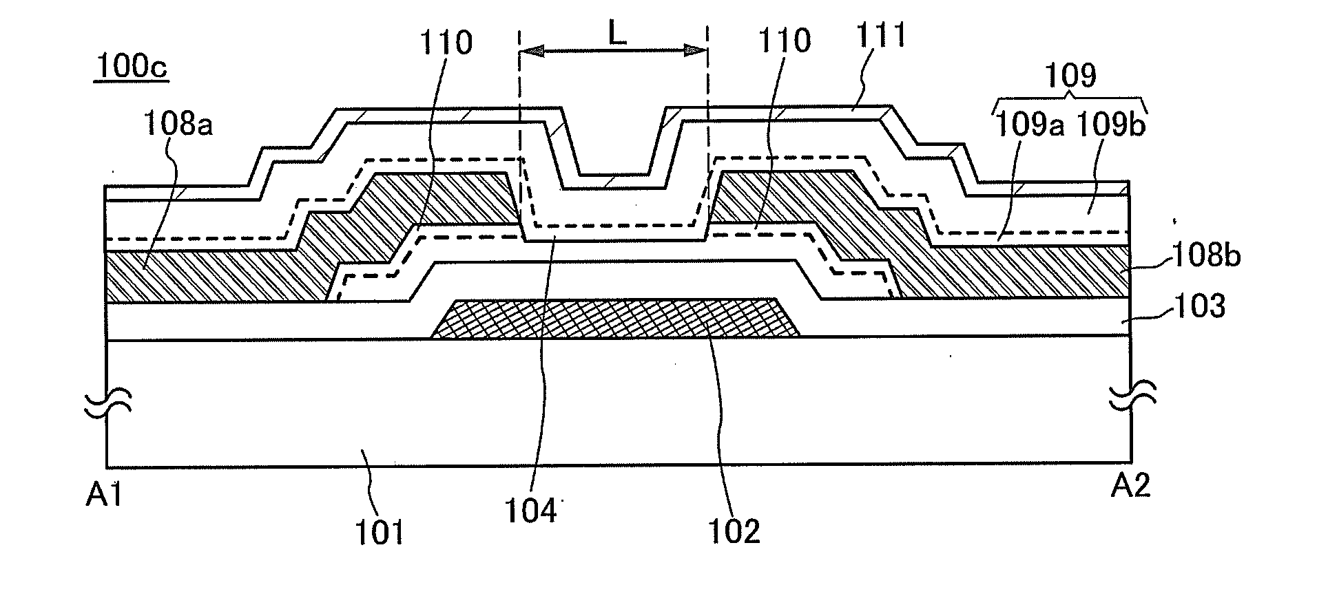
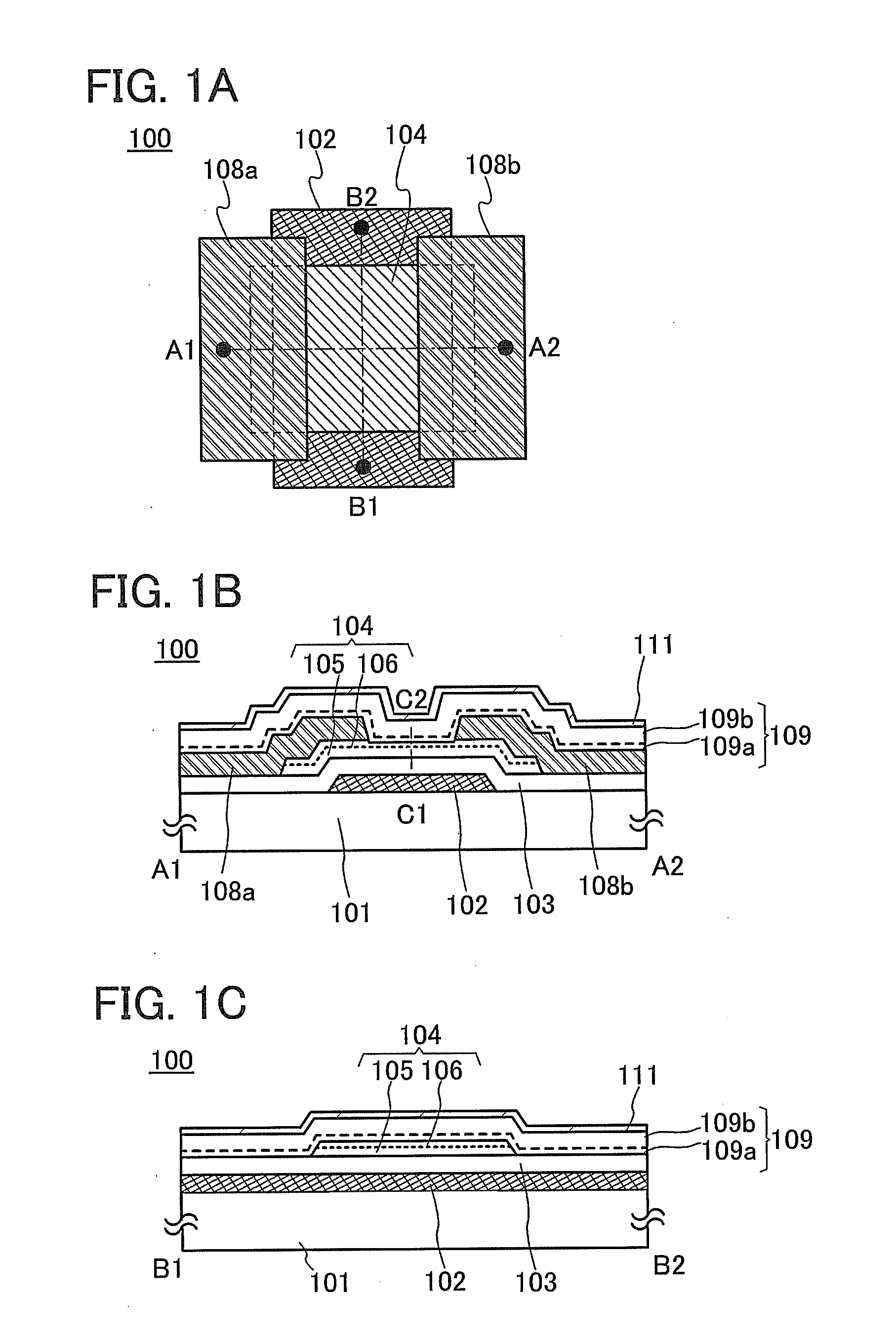
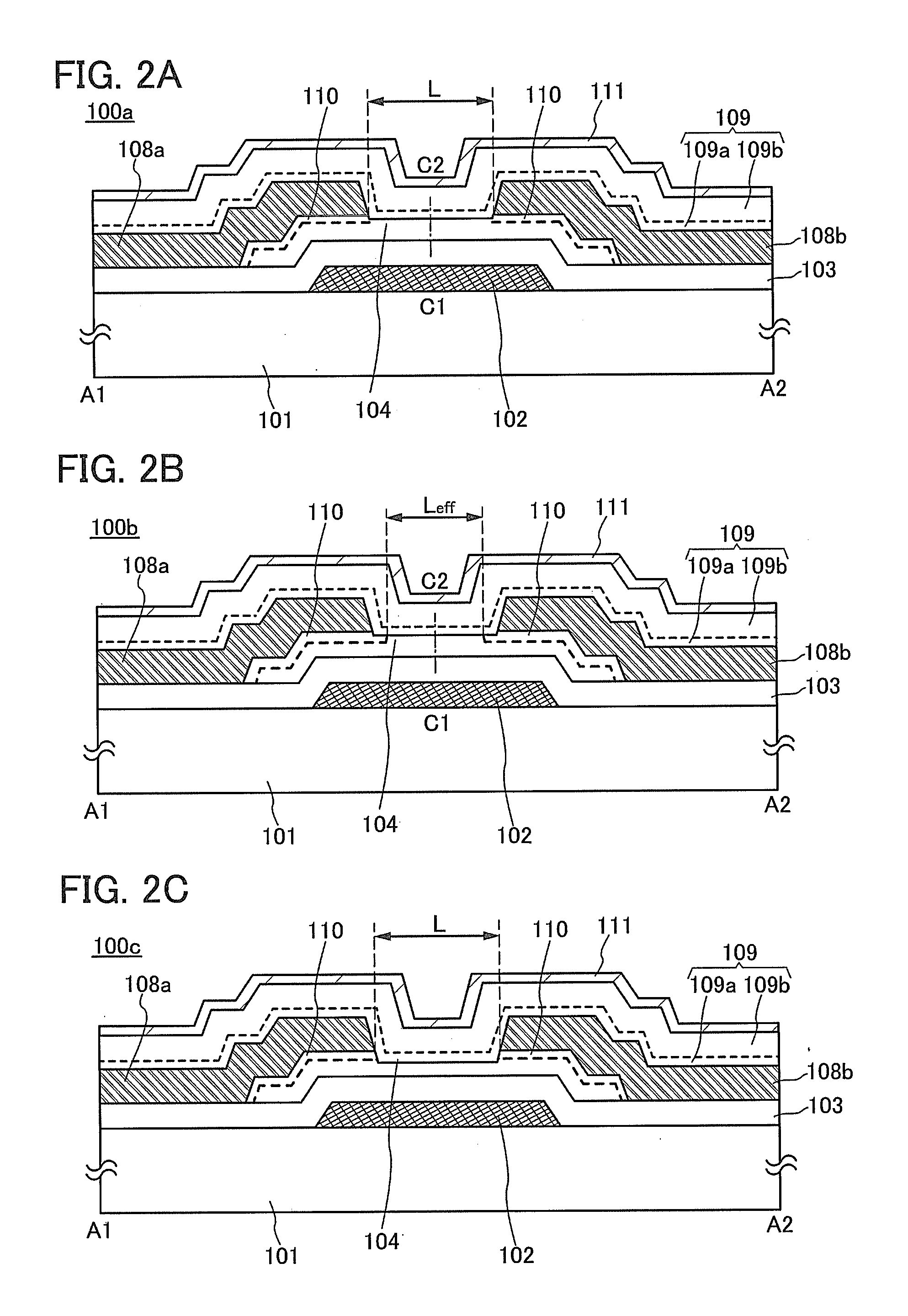
A semiconductor device including a transistor having a reduced number of oxygen vacancies in a channel formation region of an oxide semiconductor with stable electrical characteristics or high reliability is provided. A gate insulating film is formed over a gate electrode; an oxide semiconductor layer is formed over the gate insulating film; an oxide layer is formed over the oxide semiconductor layer by a sputtering method to form an stacked-layer oxide film including the oxide semiconductor layer and the oxide layer; the stacked-layer oxide film is processed into a predetermined shape; a conductive film containing Ti as a main component is formed over the stacked-layer oxide film; the conductive film is etched to form source and drain electrodes and a depression portion on a back channel side; and portions of the stacked-layer oxide film in contact with the source and drain electrodes are changed to an n-type by heat treatment.

Description

BACKGROUND OF THE INVENTION[0001]1. Field of the Invention[0002]The present invention relates to an object, a process (including a method and a manufacturing method), a machine, a manufacture, or a composition of matter. In particular, the present invention relates to, for example, a semiconductor device, a display device, a light-emitting device, a driving method thereof, or a manufacturing method thereof. The present invention particularly relates to a semiconductor device, a display device, a light-emitting device, or the like each including an oxide semiconductor.[0003]In this specification, a semiconductor device generally means a device which can function by utilizing electronic characteristics of a semiconductor, and an electrooptic device, a semiconductor circuit, and electric equipment are all included in the category of semiconductor devices.[0004]2. Description of the Related Art[0005]Semiconductor elements, for example, transistors formed using a semiconductor thin film ...

Claims


Application Information

Patent Timeline
Patent Type & Authority Applications(United States)
IPC IPC(8): H01L29/786H01L29/66H05B44/00
CPCH01L29/7869H01L29/66969H10K59/1213H01L21/32051H01L21/3213H01L21/473H01L21/4757H01L27/1225H01L29/78618H01L29/78696
Inventor YAMAZAKI, SHUNPEINAKAZAWA, YASUTAKAJINTYOU, MASAMIKOEZUKA, JUNICHIOKAZAKI, KENICHIHIROHASHI, TAKUYAADACHI, SHUNSUKE
Owner SEMICON ENERGY LAB CO LTD
Learn More