Semiconductor module for use in power supply

a technology of semiconductor modules and power supply, which is applied in the direction of semiconductor devices, semiconductor/solid-state device details, power conversion systems, etc., can solve the problems of increasing inductance, increasing the cost of electrical conductors, and increasing the number of electrical conductors to be used, so as to reduce the cost, the effect of reducing the cost of igbt modules and reducing the resistance of voltages

Active Publication Date: 2010-02-18
FUJI ELECTRIC CO LTD
View PDF4 Cites 83 Cited by
  • Summary
  • Abstract
  • Description
  • Claims
  • Application Information

AI Technical Summary

Benefits of technology

[0025]According to this invention, in the 3-phase inverter shown in FIG. 8, the IGBT series connection circuit connected to the positive terminal P and the negative terminal N of the DC power source, and IGBTs operating as the AC switch connected between the series connection point of the IGBT series connection circuit and the neutral point terminal M of the DC power source, are packaged as an integral type IGBT module, so that the wires between the respective IGBTs are not required. As a result, the wire ...

Problems solved by technology

There are disadvantages in that the number of electrical conductors to be used is large, electrical conductors having complicated shapes are required,...

Method used


Image

  • Semiconductor module for use in power supply
  • Semiconductor module for use in power supply
  • Semiconductor module for use in power supply

Examples


first embodiment

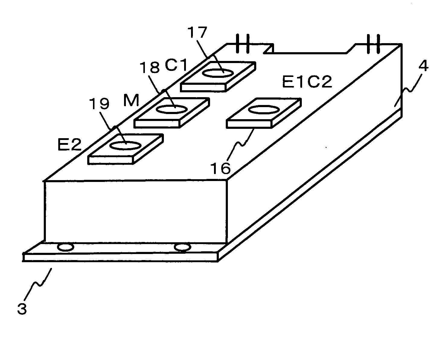
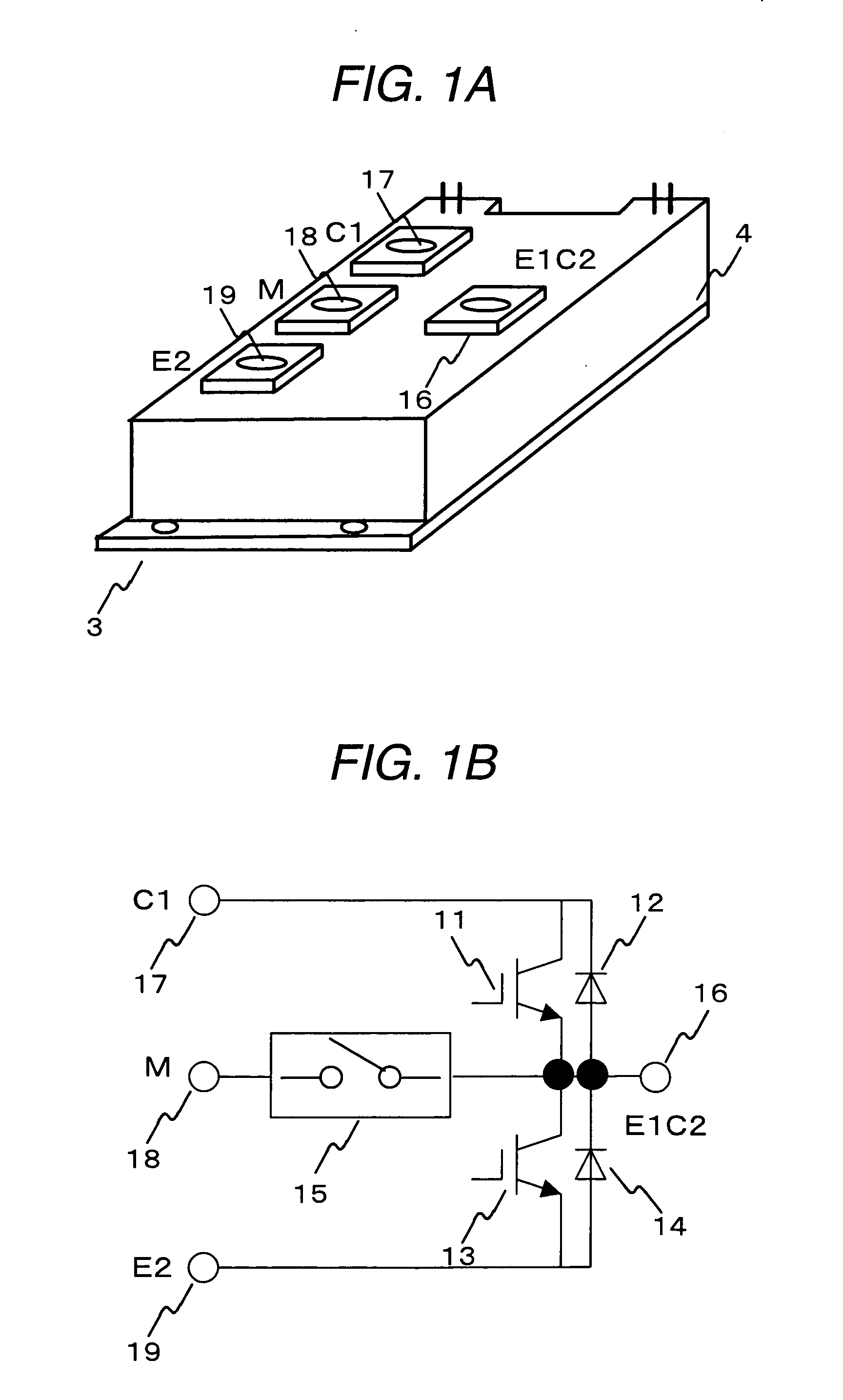
[0041]FIGS. 1A and 1B show a first embodiment of the present invention. In this embodiment, elements of one phase (in this case, the U-phase) in FIG. 8 are packaged as one module. FIG. 8 is discussed in the “Background of the Invention” section of this application. FIG. 1A shows a prospective view of the module, and FIG. 1B shows the circuit construction of the module. The elements such as IGBTs 11 and 13, diodes 12 and 14, and an AC (alternating current) switch 15 are made from semiconductor elements. A terminal 17 is a C1 terminal that receives a positive potential P of a DC power source, a terminal 18 is an M terminal that receives a neutral point potential M of the DC power source, and a terminal 19 is an E2 terminal that receives a negative potential N of the DC power source. A terminal 16 is an E1C2 terminal connected to a load. In FIG. 1A, reference numeral 3 represents a metal base substrate on which semiconductor chips and wiring members are insulated and mounted, and refer...

second embodiment

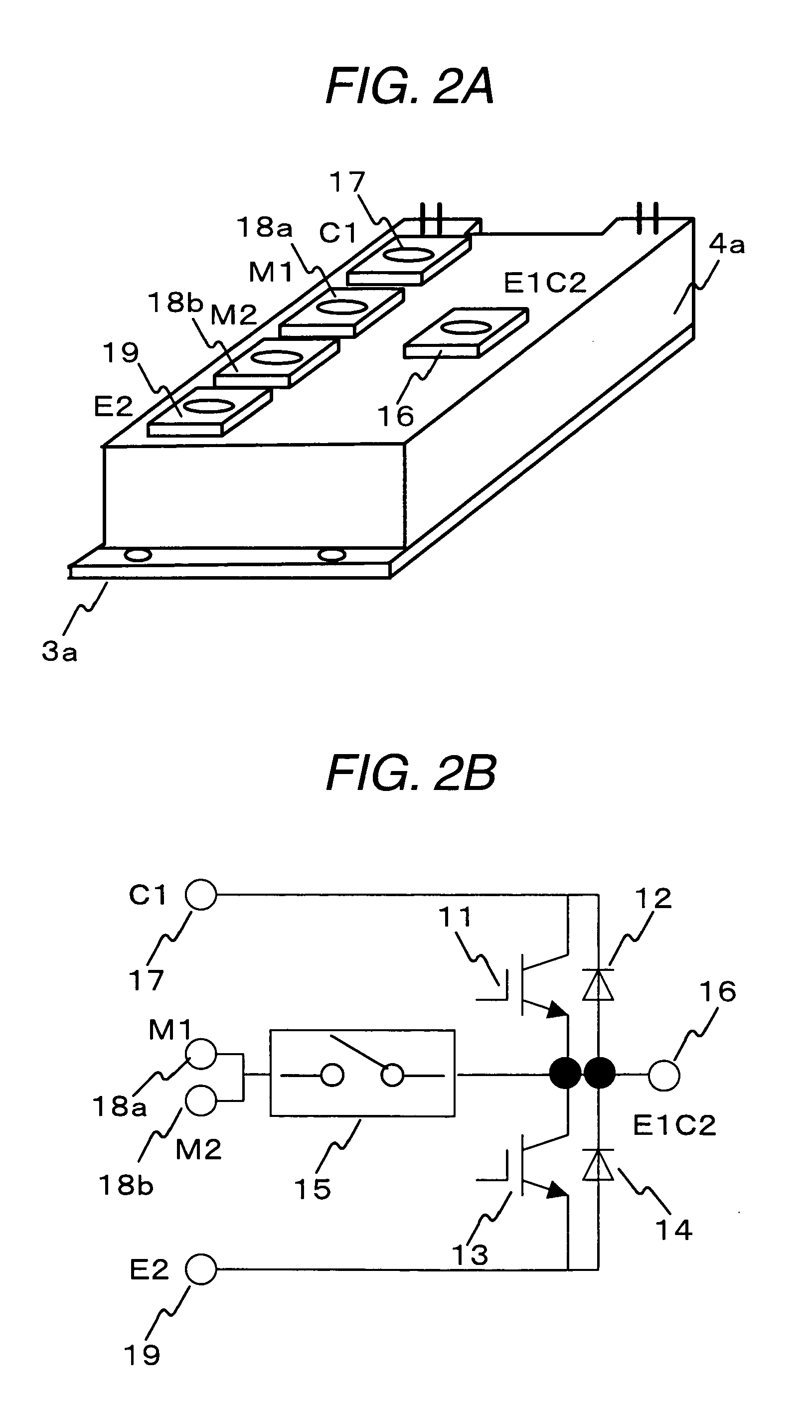
[0043]FIGS. 2A and 2B show a second embodiment of the present invention. The difference from the first embodiment resides in that the terminal connected to the neutral point potential M of the DC power source is divided into terminals M1 and M2, and the other construction is identical to that of the first embodiment. FIGS. 7A and 7B show an example of the connection between the module and the DC power source when the module of this invention is used. FIG. 7A shows the circuit construction, and FIG. 7B is a wiring diagram. By providing the module with two terminals M1 and M2, the structure of the electrical conductor 51b is simplified, and the number of steps can be reduced. In addition, the inductance can be further reduced.

third embodiment

[0044]FIGS. 3A and 3B show a third embodiment of the present invention. The elements of the three phases in FIG. 8 are packaged in one module. FIG. 3A shows the outlook of the module, and FIG. 3B shows the circuit construction. IGBTs 11, 13, 21, 23, 31, and 33, diodes 12, 14, 22, 24, 32, and 34, and AC switches 15, 25, and 35 are provided as semiconductor elements. A terminal 17 is a C1 terminal that receives the positive electrode potential P of the DC power source, a terminal 18 is an M terminal that receives the neutral point potential M of the DC power source, a terminal 19 is an E2 terminal that receives the negative electrode potential N of the DC power source. Terminals 16U, 16V, and 16W are the U, V, and W terminals connected to a three phase load. In FIG. 3A, reference numeral 3b represents a metal base substrate on which semiconductor chips and wiring members are insulated and mounted, and reference numeral 4b represents an insulating case of the module. The base substrate...


PUM


Abstract

A series connection circuit of IGBTs and an AC switch are contained in one package. The series connection circuit is connected between the positive and negative terminals of a DC power source, and the AC switch is connected between a neutral point of the DC power source and a series connection point between the IGBTs. Straight conductor strips can be used to connect terminals on the package to the DC power source, thereby reducing inductance and thus also reducing voltage spikes.

Description

BACKGROUND OF THE INVENTION[0001]1. Field of the Invention[0002]The present invention relates to the construction of a power semiconductor module used for a 3-level or 3-phase inverter or a resonance type inverter.[0003]2. Description of the Related Art[0004]FIG. 8 shows a circuit example of a 3-phase inverter for converting DC to AC, which uses a related art. The construction of this circuit is disclosed in JP-A-2002-247862. In FIG. 8, reference numerals 1 and 2 represent DC power sources connected to each other in series, and a terminal with a positive potential is represented by P, a terminal with a negative potential is represented by N, and a terminal with a neutral (middle) point potential is represented by M. In general, this DC power source may be an AC-powered DC source system, constructed by using diode rectifiers, large-capacity electrolytic capacitors, etc. (not shown).[0005]Series-connected circuits of IGBTs (insulated gate bipolar transistors), corresponding to three p...

Claims


Application Information

Patent Timeline
IPC IPC(8): H02M7/537H01L23/00
CPCH02M7/003H02M7/487H01L2924/0002H01L2924/00
Inventor TAKIZAWA, SATOKI
Owner FUJI ELECTRIC CO LTD
Why Eureka
Try Eureka