Organic light emitting device

Active Publication Date: 2010-02-25
SAMSUNG DISPLAY CO LTD
View PDF7 Cites 19 Cited by
  • Summary
  • Abstract
  • Description
  • Claims
  • Application Information

AI Technical Summary

Benefits of technology

[0009]An embodiment of the present invention includes a top-emission type organic light emitting display comprising a cathode that is transparent and ha

Problems solved by technology

However in the top-emission structure, the cathode must be transparent, which is difficult.
A conventional transparent cathode is created by forming a thin metal layer having a low work function, but the light transmittance is still very low, and it is difficult to improve light transmittance.
However, such an independent depositing method is complex, and thus the production costs increase.
Also, t

Method used


Image

  • Organic light emitting device
  • Organic light emitting device
  • Organic light emitting device

Examples


Example

Example 1

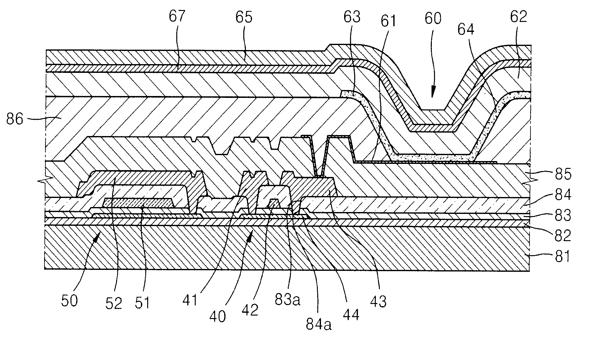
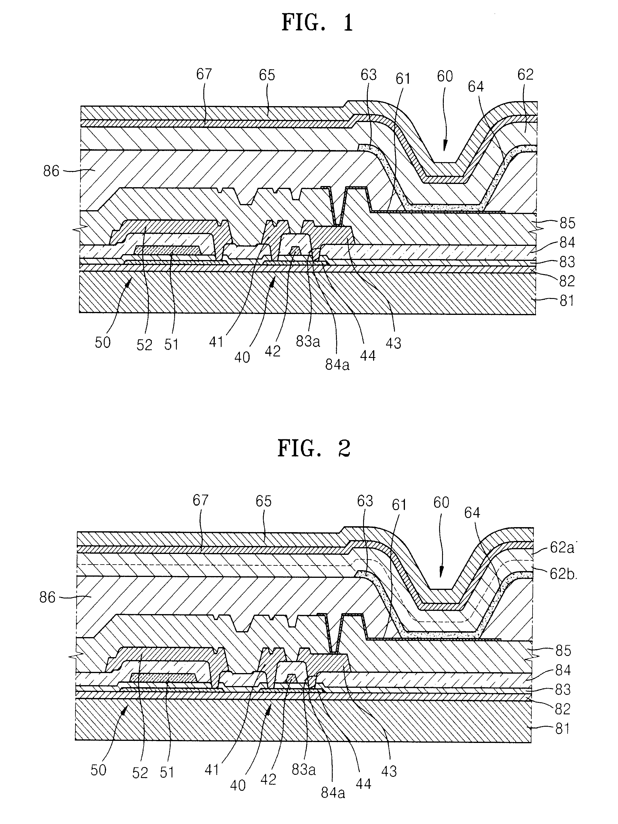
[0096]An organic light emitting display having an anode / organic layer / cathode structure was formed on a TFT as described above. In Example 1, the cathode was formed using IBAD. The ion beam used in the IBAD had a voltage of between 50 V and 200 V, and a current of between 0.05 A and 0.2 A.

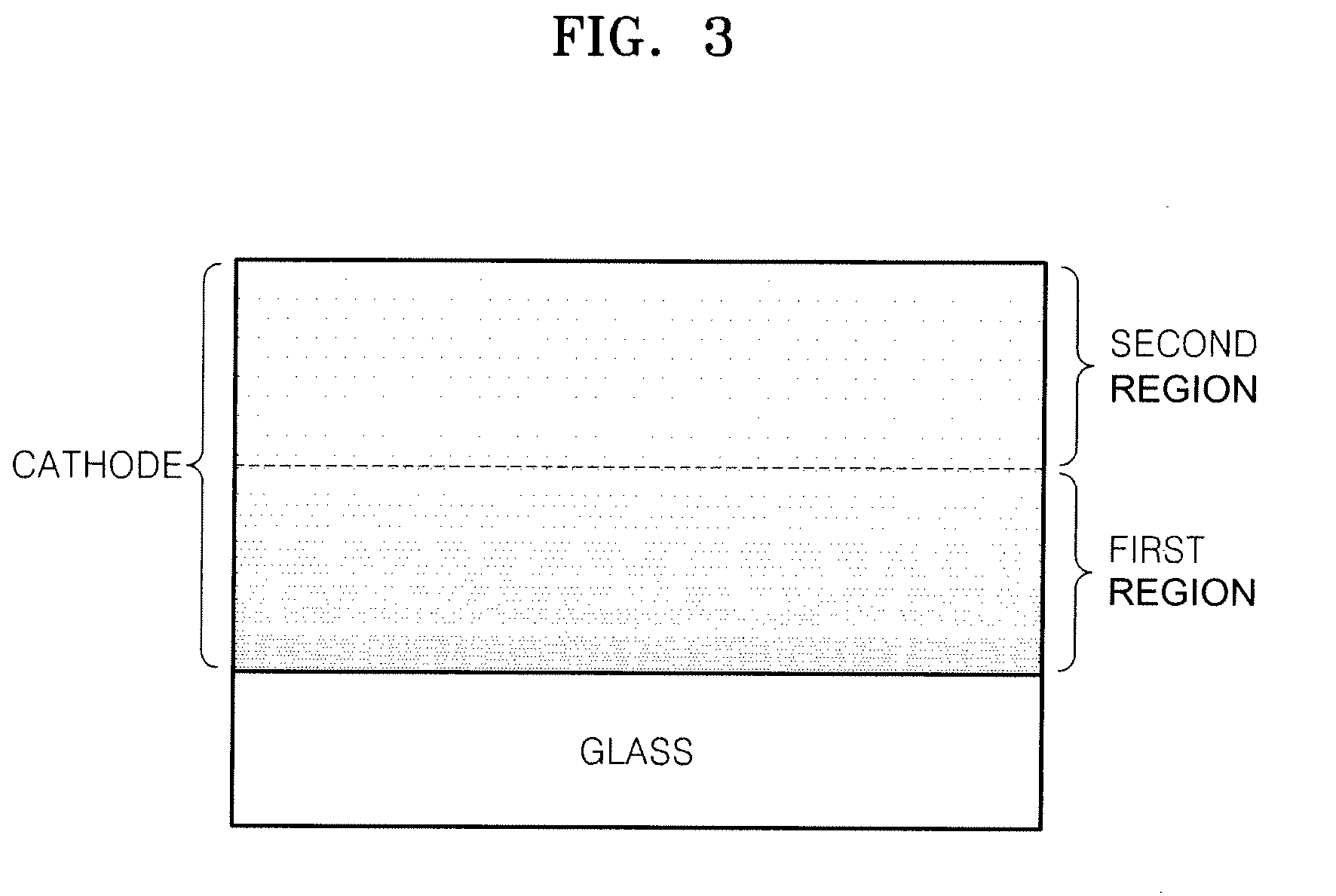
[0097]A glass substrate, wherein 1500 Å of ITO, 400 Å of 4,4′-bis(N-(4-(N-(3-methylphenyl)-N-phenylamino)phenyl)-N-phenylamino)biphenyl (DNTPD), 150 Å of NPB, 300 Å of distyrylanthracene (DSA)+5% distyrylanthraceneamine (DSAamine), 100 Å of bis(10-hydroxybenzo[h]quinolinato beryllium (Bebq2), and 10 of Å LiF were sequentially stacked on the substrate. A first layer of a cathode was formed having a thickness between 20 nm and 30 nm, by depositing calcium at an initial deposition rate of 0.7 Å / s, until the deposition rate decreased to 0.2 Å / s. Then, a second region of the cathode was formed having a thickness between 60 nm and 100 nm, by maintaining the deposition rate of calcium between 0.0...

Example

Comparative Example 1

[0099]An organic light emitting display, wherein 1500 Å of ITO, 400 Å of DNTPD, 150 Å of NPB, 300 Å of DSA+5% DSAamine, 100 Å of Bebq2, 10 Å of LiF, and 1500 Å of Al were sequentially stacked on a glass substrate in the same manner as in Example 1. The organic light emitting display made according to Comparative Example 1 is referred to as Comparative Sample 1

Evaluation

[0100]Current-voltage characteristics of Sample 1 and Comparative Sample 1 were evaluated by using a Keithley 238 source-measure unit (manufactured by Keithley Instruments, Inc.; Cleveland, Ohio). Sample 1 had an excellent current density characteristic and an excellent efficiency characteristic compared to Comparative Sample 1.

[0101]The current efficiency of Sample 1 was measured, and a current efficiency of 5 cd / A was detected at 5 V, which demonstrates that Sample 1 has excellent electric characteristics.

[0102]As described above, an organic light emitting display having a top-emission structure...


PUM

PropertyMeasurementUnit
Temperatureaaaaaaaaaa
Fractionaaaaaaaaaa
Fractionaaaaaaaaaa

Abstract

An organic light emitting display includes an anode; an organic layer on the anode; and a cathode on the organic layer. The cathode includes a first region and a second region which are sequentially disposed on the organic layer in parallel. The first and second regions are formed by doping a metal oxide on an indium oxide matrix. The doping density of the metal oxide of the first region is greater than that of the second region, the metal oxide of the first region has a density gradient, and the density of the metal oxide in a boundary surface of the first and second regions is the same. An organic light emitting display according to the present invention can increase light emitting efficiency without using a resonance structure.

Description

CROSS-REFERENCE TO RELATED PATENT APPLICATION[0001]This application claims priority to and the benefit of Korean Patent Application No. 10-2008-0081363, filed in the Korean Intellectual Property Office on Aug. 20, 2008, the entire content of which is incorporated herein by reference.FIELD OF THE INVENTION[0002]The present invention relates to an organic light emitting display having a top-emission structure with improved light emitting efficiency.BACKGROUND OF THE INVENTION[0003]Organic light emitting displays are self-emission devices. Organic light emitting displays have higher luminescence than liquid crystal displays, and are thinner than liquid crystal displays, as organic light emitting displays do not include a backlight unit.[0004]An organic light emitting display has a structure wherein an anode, an organic layer, and a cathode are sequentially stacked on a substrate on which a pixel circuit, such as a thin film transistor, is deposited. The structure of an organic light em...

Claims


Application Information

Patent Timeline
IPC IPC(8): H01J1/62B05D5/12C23C14/48
CPCH01L27/3244H01L27/3276Y10S428/917H01L51/5234H01L2251/5315H01L51/5221H10K59/12H10K59/131H10K50/828H10K2102/3031H10K2102/3026H10K50/82H10K2102/351
Inventor KIM, YONG-TAKLEE, JONG-HYUKKIM, WON-JONGLEE, JOON-GUCHOI, JIN-BAEK
Owner SAMSUNG DISPLAY CO LTD
Why Eureka
Try Eureka