Smooth and vertical semiconductor fin structure

a semiconductor fin and vertical technology, applied in the direction of semiconductor devices, basic electric elements, electrical equipment, etc., can solve the problems of large difficulty in maintaining performance improvement of devices of deeply submicron generation, and the complexity of technology

Inactive Publication Date: 2010-02-25
GLOBALFOUNDRIES INC
View PDF17 Cites 336 Cited by
  • Summary
  • Abstract
  • Description
  • Claims
  • Application Information

AI Technical Summary

Problems solved by technology

As FET (Field-Effect-Transistor) devices are being scaled down, the technology becomes more complex, and changes in device structures and new fabrication methods are needed to maintain th

Method used


Image

  • Smooth and vertical semiconductor fin structure
  • Smooth and vertical semiconductor fin structure
  • Smooth and vertical semiconductor fin structure

Examples


Embodiment Construction

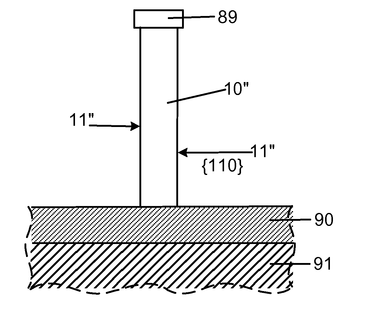
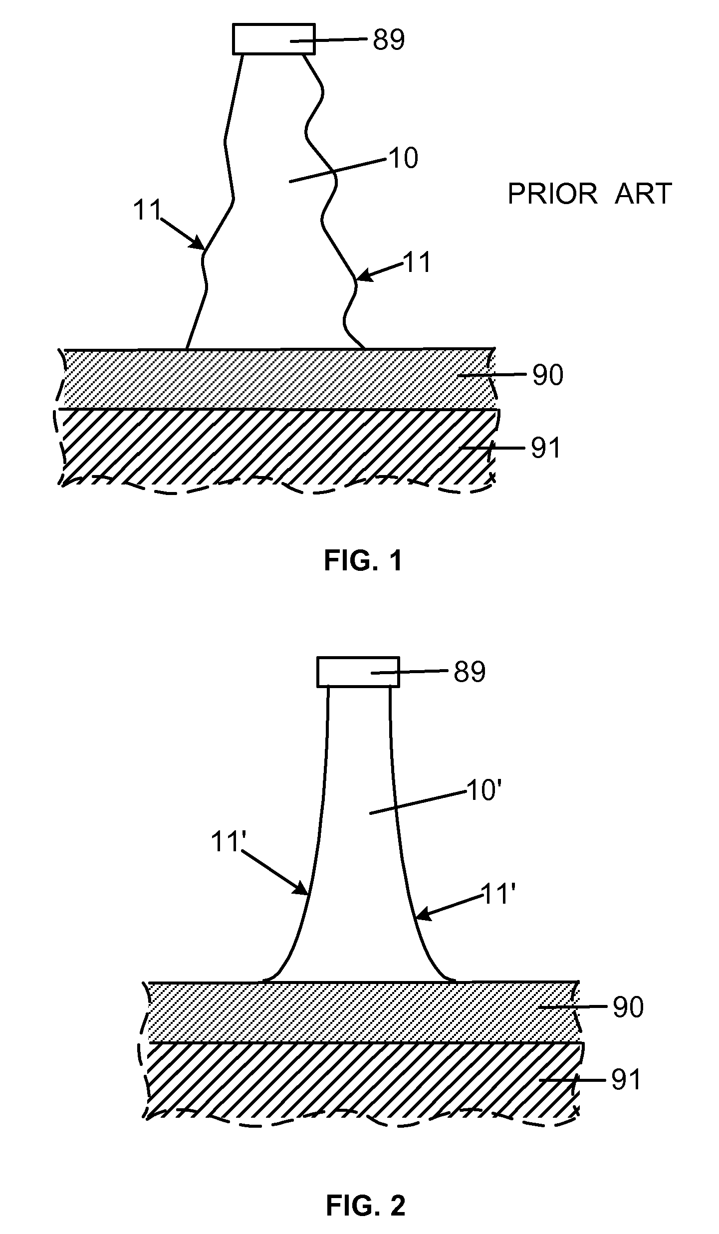
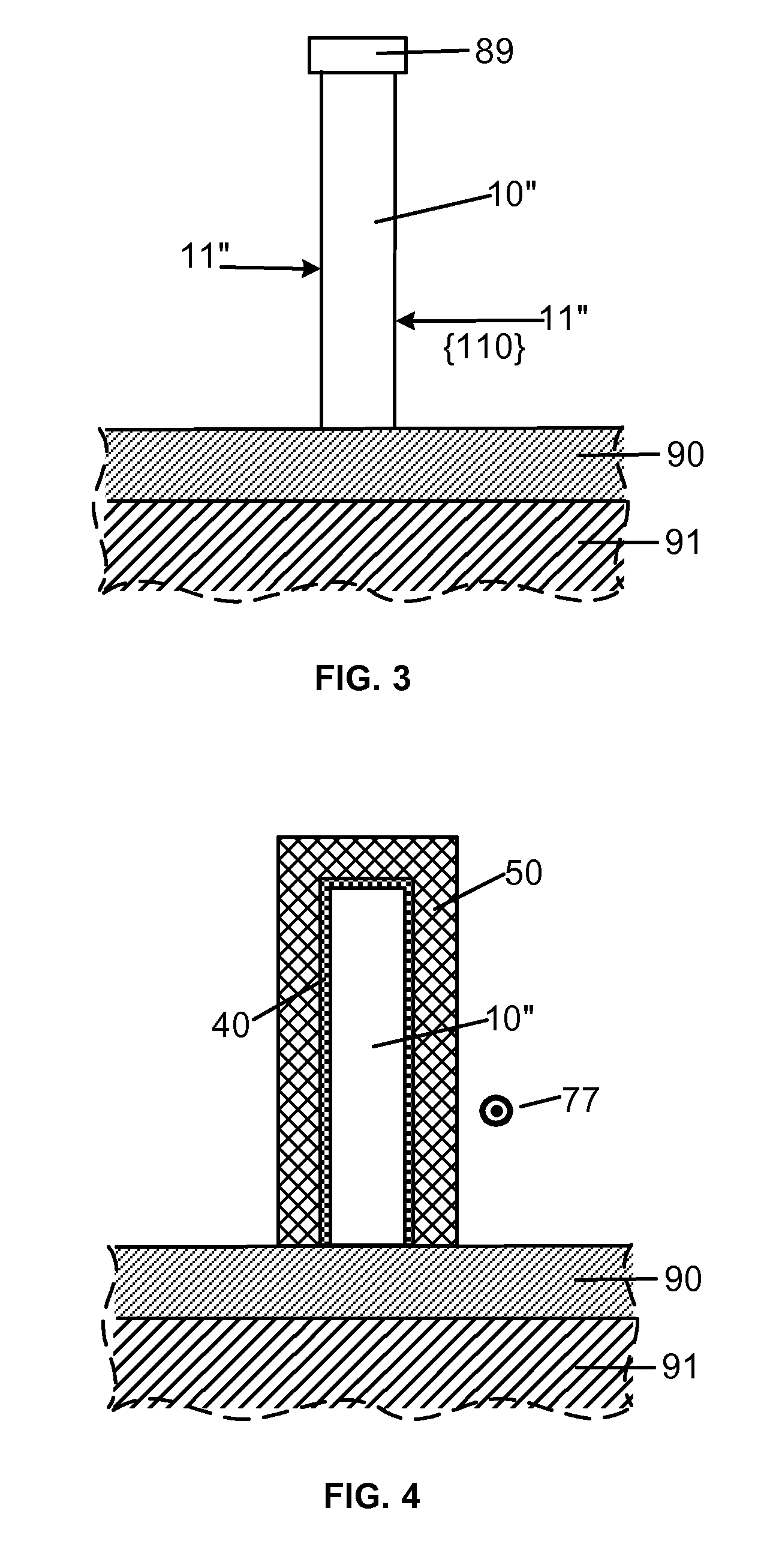
[0011]It is understood that Field Effect Transistors (FETs) are well known in the electronic arts. Standard components of a FET are the source, the drain, the body in-between the source and the drain, and the gate. The body is usually part of a substrate, and it is often called substrate. The gate is overlaying the body and is capable to induce a conducting channel in the body between the source and the drain. In the usual nomenclature, the channel is hosted by the body. The gate is separated from the body by the gate insulator, or dielectric. The FET source and drain are often referred to simply as electrodes. The electrodes adjoin the induced conductive channel and are capable of being in electrical continuity with the induced conductive channel.

[0012]A type of FET device known in the art is the so called FinFET device, having a fin-type body. The fin-type body is a fin structure, standing out of a planar surface. Such FET devices, with fin-type bodies, have several advantages as ...


PUM


Abstract

A method for processing a semiconductor fin structure is disclosed. The method includes thermal annealing a fin structure in an ambient containing an isotope of hydrogen. Following the thermal annealing step, the fin structure is etched in a crystal-orientation dependent, self-limiting, manner. The crystal-orientation dependent etch may be selected to be an aqueous solution containing ammonium hydroxide (NH4OH). The completed fin structure has smooth sidewalls and a uniform thickness profile. The fin structure sidewalls are {110} planes.

Description

FIELD OF THE INVENTION[0001]The present invention relates to devices used in integrated circuits, and to their manufacturing. More particularly, the present invention relates to improving the performance of FinFET devices.BACKGROUND OF THE INVENTION[0002]Today's integrated circuits include a vast number of devices. Smaller devices and shrinking ground rules are the key to enhance performance and to reduce cost. As FET (Field-Effect-Transistor) devices are being scaled down, the technology becomes more complex, and changes in device structures and new fabrication methods are needed to maintain the expected performance enhancement from one generation of devices to the next. The mainstay material of microelectronics is silicon (Si), or more broadly, Si based materials. One such Si based material of importance for microelectronics is the silicon-germanium (SiGe) alloy. The structures and devices in the embodiments of the present disclosure are typically part of the art of single-crystal...

Claims


Application Information

Patent Timeline
IPC IPC(8): H01L21/302
CPCH01L21/30608H01L29/66795H01L29/045
Inventor CHENG, KANGGUODORIS, BRUCE B.FALTERMEIER, JOHNATHAN E.ZHANG, YING
Owner GLOBALFOUNDRIES INC
Why Eureka
Try Eureka