Supercharge Your Innovation With Domain-Expert AI Agents!

Memory management system and method thereof

Active Publication Date: 2010-02-25
SONIX TECH
View PDF6 Cites 3 Cited by
  • Summary
  • Abstract
  • Description
  • Claims
  • Application Information

AI Technical Summary

Benefits of technology

[0006]In light of the above-mentioned problem, one object of the invention is to provide a memory management system and a method thereof to reduce the number of physical address lines, increase the flexibility in memory expansion, and reduce the production cost.
[0011]The memory management system and the related management method are to partition the first memory into a normal access memory bank and at least one switching access memory bank. The secondary data bank of the secondary memory is read / written together with mapping the switching access memory bank. By such approach, the memory management system and the related management method according to the invention allow a user or designer expanding the number of addressable addresses and the memory space without limitation, even within the limited memory addressable range. Therefore, reducing the number of pins required for memory addressing, expanding the memory space flexibly, and reducing the overall system cost can be achieved.

Problems solved by technology

In most practical applications, the size of the memory in a microprocessor system is often limited by the addressable address range of the microprocessor system and cannot be increased.
Therefore, the functionality of the microprocessor system is also limited.
The size of the memory is limited by the addressable address range of the microprocessor and the cost of the overall system.
Therefore, under suitable considerations in the various factors, how to provide the largest memory resource utilized by the system becomes a very important issue.

Method used


Image

  • Memory management system and method thereof
  • Memory management system and method thereof
  • Memory management system and method thereof

Examples


Embodiment Construction

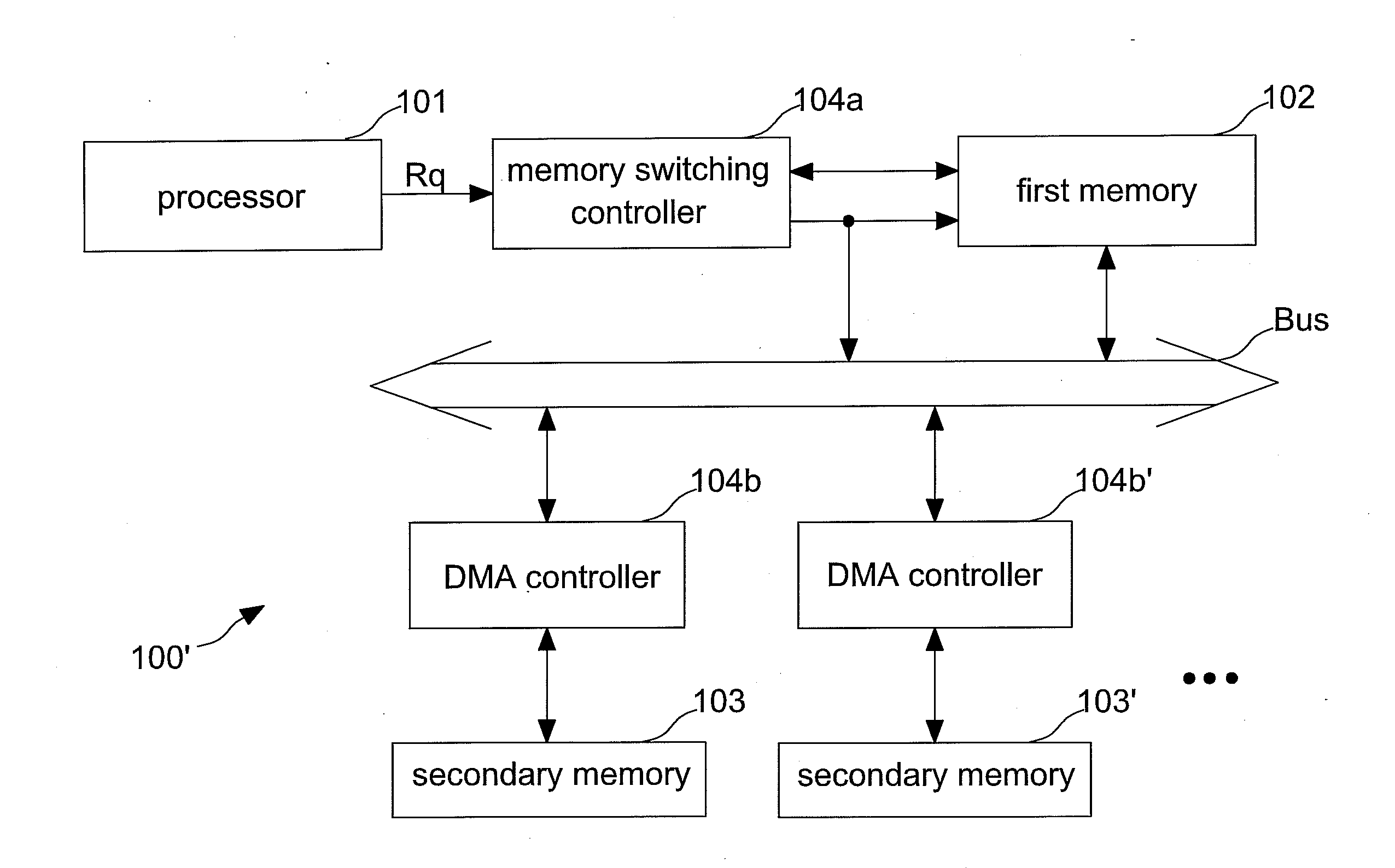
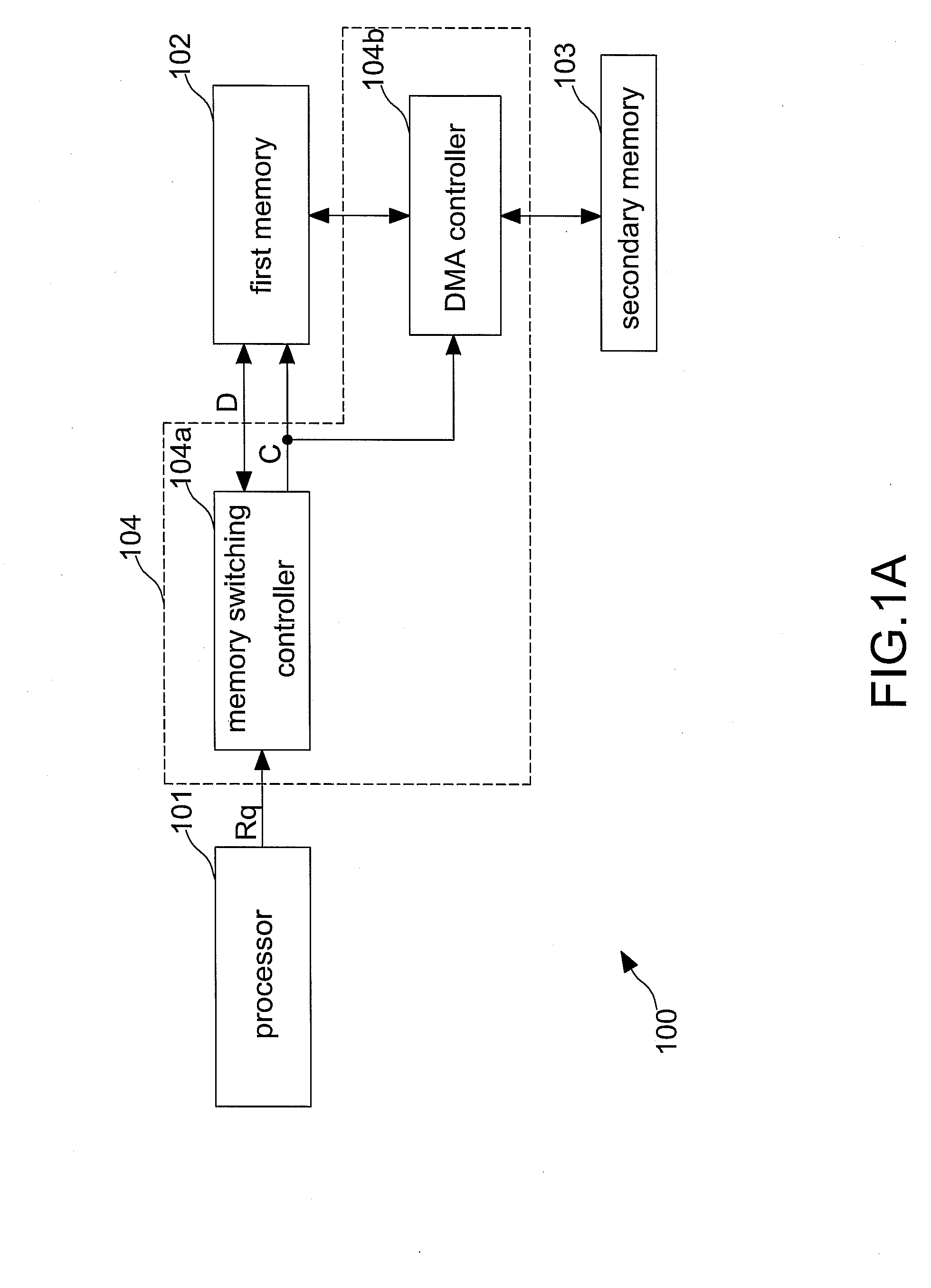
[0016]FIG. 1A shows a schematic diagram illustrating the memory management system according to one embodiment of the invention. The memory management system 100 includes a processor 101, a first memory 102, a secondary memory 103, and a memory management device 104.

[0017]The processor 101 can be a central processing unit (CPU), a microprocessor unit (MPU), a microprocessor control unit (MCU), or any other current existing processing device, or any future-developed processing device. The processor 101 issues a request signal Rq to access data in the memory.

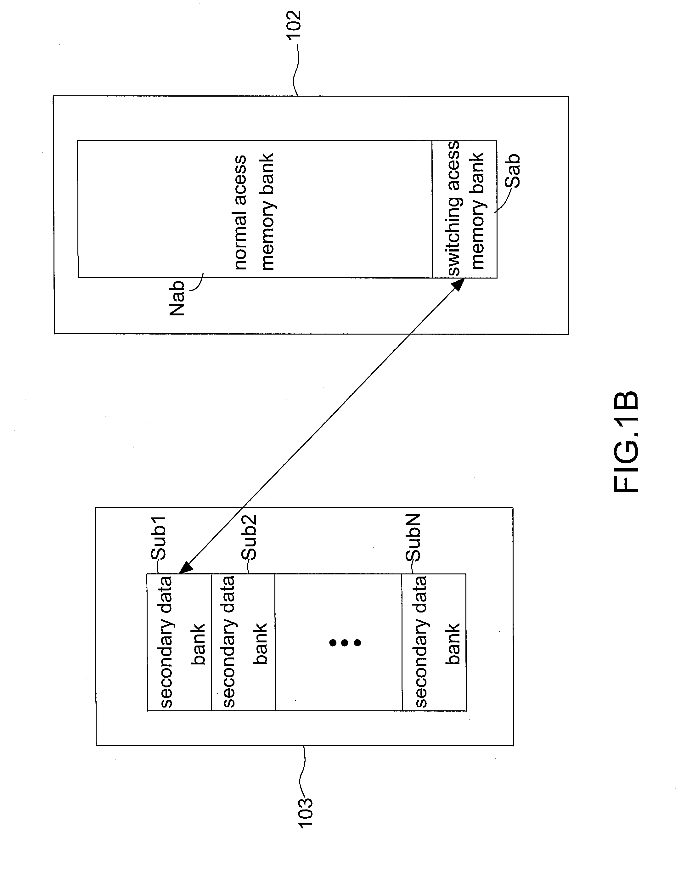
[0018]The first memory 102 can be a static random access memory (SRAM), any current existing memory, or any future-developed memory. The first memory 102 includes a normal access memory bank and at least one switching access memory bank. The memory space of the first memory 102, shown in FIG. 1B, according to one embodiment of the invention includes a normal access memory bank Nab and a switching access memory bank Sab. Although th...


PUM


Abstract

The invention discloses a memory management system and a memory management method are disclosed. The memory management system includes a first memory, at least one secondary memory, and a memory management device. The first memory includes a normal access memory bank and at least one switching access memory bank. The secondary memory includes at least one secondary access memory bank corresponding to the switching access memory bank. The memory management device reads / writes the normal access memory bank or the secondary access memory bank.

Description

BACKGROUND OF THE INVENTION[0001](a) Field of the Invention[0002]The present invention relates to memory access technology, and more particularly, to a memory management system and a method thereof.[0003](b) Description of the Related Art[0004]The addressable address range of a common microprocessor system is limited by the number of address lines in the address bus thereof. Taking the currently available digital system as an example, the addressable address range of the microprocessor is equal to two to the power of the number of the address lines. For example, the addressable address range of sixteen address lines is equal to two to the power of sixteen (216), 65536 addresses. However, due to considerations in the architecture and the cost, the number of address lines is reduced as much as possible in a most 8-bit microprocessor system. In most practical applications, the size of the memory in a microprocessor system is often limited by the addressable address range of the micropr...

Claims


Application Information

Patent Timeline
IPC IPC(8): G06F13/00G06F12/00
CPCG06F12/0623G06F12/08G06F2212/1048G06F13/28G06F13/1684
Inventor KAO, CHIEN-LONGHSIN, YI-CHIH
Owner SONIX TECH
Features
  • R&D
  • Intellectual Property
  • Life Sciences
  • Materials
  • Tech Scout
  • Unparalleled Data Quality
  • Higher Quality Content
  • 60% Fewer Hallucinations
Learn More