Light-emitting device, electronic equipment, and process of producing light-emitting device

Inactive Publication Date: 2010-03-04
SEIKO EPSON CORP
View PDF10 Cites 81 Cited by
  • Summary
  • Abstract
  • Description
  • Claims
  • Application Information

AI Technical Summary

Benefits of technology

[0008]An advantage of some aspects of the invention is to provide a cathode having both a high electrical conductivity and a high transparency and a

Problems solved by technology

Therefore, the reduction in the thickness causes a problem that the electrical conductivity of the light-emitting element is decreased.
However, in such a case, there is a possibility that asperities are generated by aggregation of the Ag atoms, and if a layer for absorbing the effect of such asperities is additionally formed, ther

Method used


Image

  • Light-emitting device, electronic equipment, and process of producing light-emitting device
  • Light-emitting device, electronic equipment, and process of producing light-emitting device
  • Light-emitting device, electronic equipment, and process of producing light-emitting device

Examples


first embodiment

A: First Embodiment

A-1 Structure of Light-Emitting Device

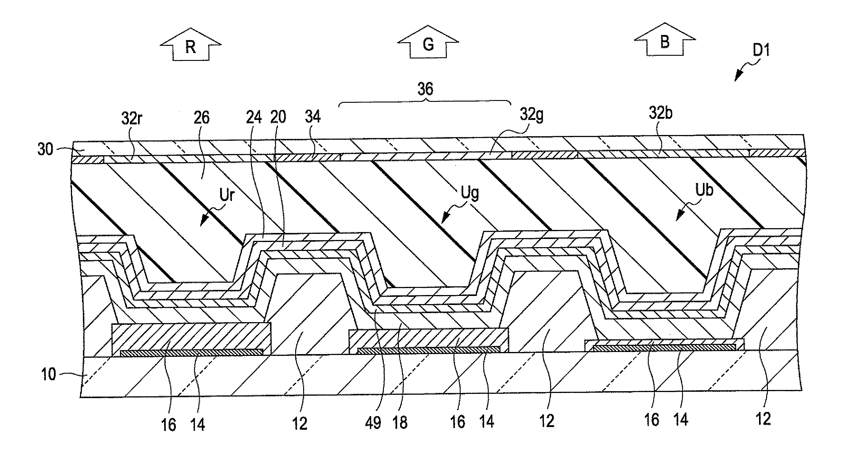
[0088]FIG. 1 is a cross-sectional view illustrating a structure of a light-emitting device D1 according to a first embodiment of the invention. As shown in FIG. 1, the light-emitting device D1 is configured such that a plurality of light-emitting elements U (Ur, Ug, and Ub) is arrayed on a surface of a first substrate 10. Each of the light-emitting elements U is an element generating light with a wavelength corresponding to any of a plurality of colors (red, green, and blue). In these elements, a single light-emitting function layer is common to the plurality of elements, and emission light with a wavelength corresponding to the respective light-emitting elements is extracted by controlling the optical length between the below-described reflecting layer and semi-reflective opposite electrode in each light-emitting element for optimizing resonance. In the first embodiment, by the resonance effect, the light-emitting element Ur ...

second embodiment

B: Second Embodiment

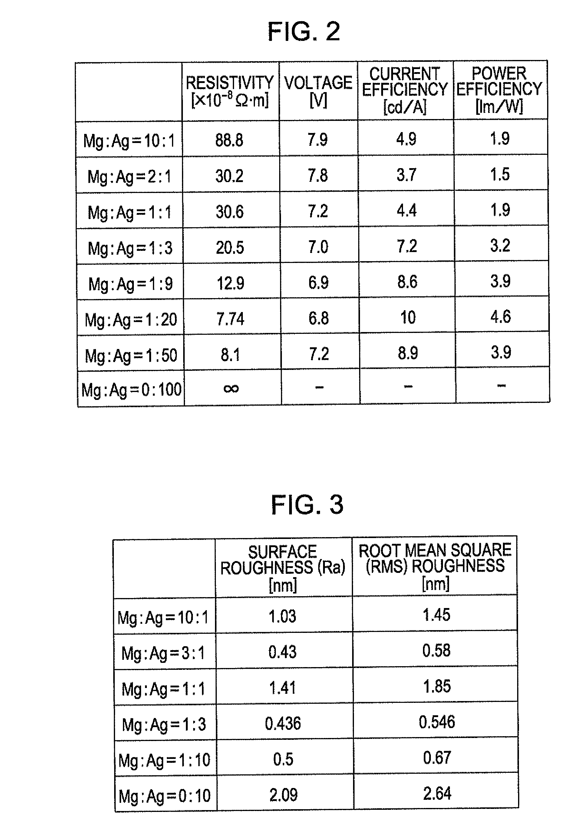
[0130]In a second embodiment, the deposition rate ratio of Mg and Ag for forming the opposite electrode 20 is set to 1:9. Since the other configuration is the same as that of the first embodiment, the description thereof is omitted,

[0131]FIG. 11 is a diagram showing measurement results of various factors in each case that the thickness of the opposite electrode 20 of the light-emitting element Ug according to the second embodiment is 10 nm, 13 nm, or 16 nm, The sheet resistance values shown in FIG. 11 are those of the opposite electrode 20, and the values of voltage, current efficiency, and power efficiency are those when the density of current flowing in the opposite electrode 20 is set to 17.5 mA / cm2. In addition, though it is not shown in the drawing, the values of the various factors when the thickness of the opposite electrode 20 is 20 nm are equivalent to those when the thickness is 16 nm.

[0132]As shown in FIG. 11, it is confirmed that the sheet resistance ...

third embodiment

C: Third Embodiment

[0133]FIG. 12 is a cross-sectional view illustrating a structure of a light-emitting device D2 according to a third embodiment of the invention. In the above-described embodiments, the light-emitting function layer 18 is common to all the light-emitting elements U, but in the third embodiment, the light-emitting function layer 18 is independently formed for each emission color of the light-emitting elements U.

[0134]As shown in FIG. 12, the light-emitting function layers 18 (18r, 18g, and 18b) each include a hole-injection layer 41 disposed on the pixel electrode 16, a hole-transporting layer 43 disposed on the hole-injection layer 41, a light-emitting layer 45 (45r, 45g, or 45b) disposed on the hole-transporting layer 43, and an electron-transporting layer 47 disposed on the light-emitting layer 45. The light-emitting function layer 18r of the light-emitting element Ur contains the light-emitting layer 45r made of an organic EL material that generates light of an ...


PUM


Abstract

A light-emitting device includes a light-reflecting layer, a first electrode disposed on or above the light-reflecting layer, a semi-transparent reflective second electrode, a light-emitting function layer disposed between the first electrode and the second electrode, and an electron-injection layer disposed between the light-emitting function layer and the second electrode. The second electrode is made of an Ag alloy having an Ag content of from 50% by atoms to 98% by atoms.

Description

BACKGROUND[0001]1. Technical Field[0002]The present invention relates to a light-emitting device, electronic equipment, and a process of producing the light-emitting device.[0003]2. Related Art[0004]Recently, various types of light-emitting devices having light-emitting elements such as organic EL (electroluminescent) elements or organic light-emitting diodes (hereinafter, referred to as “OLEDs”) called light-emitting polymer elements are proposed. The light-emitting elements included in such light-emitting devices usually have a structure in which a light-emitting layer made of an organic EL material is disposed between two electrodes.[0005]For example, Japanese Patent No. 2723242 (Patent Document 1) discloses a light-emitting element composed of an anode, an organic light-emitting medium disposed on the anode, and a cathode disposed on the organic light-emitting medium. In Patent Document 1, a portion of the organic light-emitting medium in contact with the anode functions as a ho...

Claims


Application Information

Patent Timeline
IPC IPC(8): H01L33/00
CPCH01L51/5036H01L51/5092H01L51/5206H01L2251/558H01L51/5237H01L51/5265H01L2251/5315H01L51/5234H10K59/30H10K50/125H10K50/171H10K50/81H10K50/824H10K50/828H10K50/8426H10K50/852H10K50/844H10K2102/3026H10K2102/351H10K71/00H10K50/84H10K50/805H10K50/818H10K50/856H10K71/60
Inventor KOBAYASHI, HIDEKAZUSHIRATORI, KOYAYOSHIOKA, ATSUSHI
Owner SEIKO EPSON CORP
Why Eureka
Try Eureka