[0015]The first preferred display device offers the same advantageous effects as those of a display device according to the first aspect of the invention described above. Moreover, with such a preferred configuration, the first preferred display device makes it possible to conduct a display lighting test and a
low resistance short test for each color.
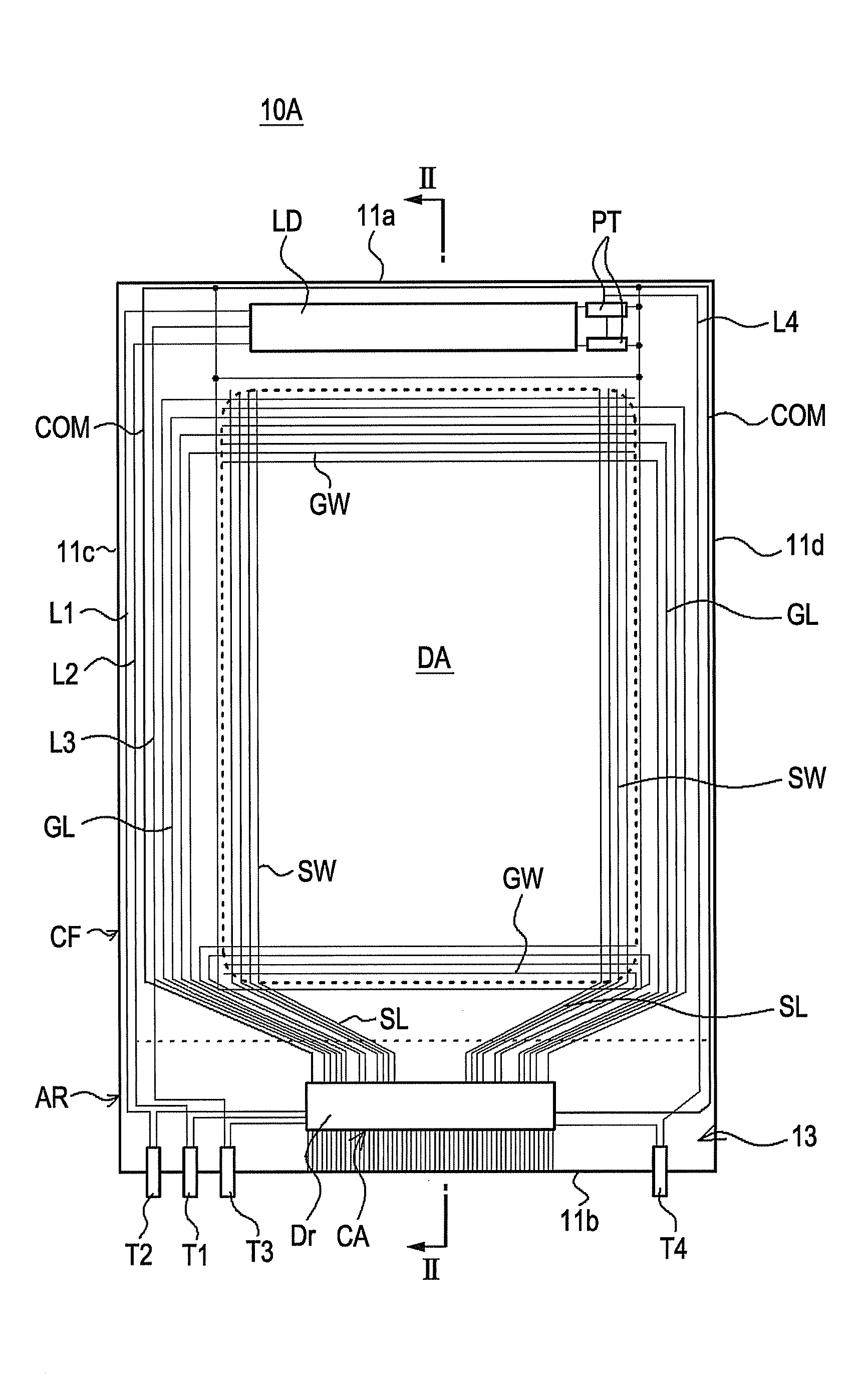
[0016]In the configuration of a display device according to the first aspect of the invention described above or the first preferred display device described above, it is preferable that the plurality of scanning lines should be divided into four groups, which are a first scanning line group, a second scanning line group, a third scanning line group, and a fourth scanning line group; the plurality of scanning lines should extend to the lead part for each of the first scanning line group, the second scanning line group, the third scanning line group, and the fourth scanning line group; and the testing terminals connected respectively to the plurality of scanning lines should be separately arrayed near one another so as to correspond to the first scanning line group, the second scanning line group, the third scanning line group, and the fourth scanning line group. A display device having the preferred configuration described above may be hereafter referred to as “the second preferred display device”.
[0017]The second preferred display device offers the same advantageous effects as those of a display device according to the first aspect of the invention described above. Moreover, with such a preferred configuration, the second preferred display device makes it possible to conduct a display lighting test and a
low resistance short test for each of four scanning line groups.
[0018]It is preferable that the second preferred display device should further include a first switching element and a second switching element each of which is provided in the lead part, wherein the light sensor element
control line is connected to a first
electrode of the first switching element; the electrostatic protection element
control line is connected to a first
electrode of the second switching element; a testing terminal is connected to a second
electrode of the first switching element; another testing terminal is connected to a second electrode of the second switching element; still another testing terminal is connected to a control electrode of the first switching element; still another testing terminal is connected to a control electrode of the second switching element; the testing terminals of the light sensor element
signal lines are arrayed adjacent to two testing terminals of the plurality of
signal lines, respectively; and the testing terminals that are connected to the second electrodes of the first switching element and the second switching element and to the control electrodes of the first switching element and the second switching element are arrayed separately in such a manner that each of the testing terminals that are connected to the second electrodes of the first switching element and the second switching element and to the control electrodes of the first switching element and the second switching element is provided adjacent to an array of the testing terminals of the corresponding one of the first scanning line group, the second scanning line group, the third scanning line group, and the fourth scanning line group. A display device having the preferred configuration described above may be hereafter referred to as “the third preferred display device”.
[0019]In such a preferred configuration of the third preferred display device, it is possible to switch the first switching element and the second switching element into an ON / OFF state by varying a
voltage that is applied to each of four scanning line groups. When the first switching element and the second switching element are set in an ON state, the control electrode of the light sensor element and the control electrode of the electrostatic protection element are electrically connected to any of four scanning line groups. Therefore, it is possible to conduct a low resistance short test and a lighting test of the display device. The third preferred display device offers the same advantageous effects as those of the second preferred display device described above. Moreover, with such a preferred configuration, the third preferred display device makes it possible to detect a short circuit between the control electrode of the light sensor element and the
common line as well as a short circuit between the control electrode of the electrostatic protection element and the
common line.
[0020]It is preferable that the second preferred display device should further include a first switching element, a second switching element, a third switching element, and a fourth switching element each of which is provided in the lead part, wherein the light sensor element
control line is connected to a first electrode of the first switching element and to a first electrode of the third switching element; the electrostatic protection element control line is connected to a first electrode of the second switching element and to a first electrode of the fourth switching element; a testing terminal is connected to a second electrode of the first switching element; another testing terminal is connected to a second electrode of the second switching element; still another testing terminal is connected to a second electrode of the third switching element; still another testing terminal is connected to a second electrode of the fourth switching element; shared testing terminals are connected to control electrodes of the first switching element, the second switching element, the third switching element, and the fourth switching element; the testing terminals of the light sensor element
signal lines are arrayed adjacent to two testing terminals of the plurality of
signal lines, respectively; any two terminals among the testing terminals that are connected to the second electrodes of the first switching element, the second switching element, the third switching element, and the fourth switching element are arrayed adjacent to the testing terminal of the
common line; and the remaining two terminals among the testing terminals that are connected to the second electrodes of the first switching element, the second switching element, the third switching element, and the fourth switching element as well as the shared testing terminals that are connected to the control electrodes of the first switching element, the second switching element, the third switching element, and the fourth switching element are arrayed separately in such a manner that each one of the remaining two and shared terminals mentioned above is provided adjacent to an array of the testing terminals of the corresponding one of the first scanning line group, the second scanning line group, the third scanning line group, and the fourth scanning line group. A display device having the preferred configuration described above may be hereafter referred to as “the fourth preferred display device”.

