Phase Detector Circuit for Clock and Data Recovery Circuit and Optical Communication Device Having the Same

a phase detector and clock technology, applied in the direction of digital transmission, synchronisation signal speed/phase control, instruments, etc., can solve the problems of increasing circuit power consumption, difficult to invert the polarity of an analog voltage value with high accuracy,

Inactive Publication Date: 2010-03-04
HITACHI LTD
View PDF10 Cites 15 Cited by
  • Summary
  • Abstract
  • Description
  • Claims
  • Application Information

AI Technical Summary

Benefits of technology

[0016]The present invention makes it possible, as a typical advantageous effect thereof, to realize a small-sized, low-power-consuming, high-accuracy, track-and-hold type phase detector circuit compatible with a 1 / N rate architecture. As another typical advantageous effect of the invention, a communication device including a serializer / deserializer in which a CDR circuit having a track-and-hold type phase detector circuit according to the invention is used and in which N-phase clock signals each having a period equaling N times a symbol time are used can be made producible at a low cost compared with an existing type of a communication device, and the communication device can be also made low-power-consuming.
, a communication device including a serializer / deserializer in which a CDR circuit having a track-and-hold type phase detector circuit according to the invention is used and in which N-phase clock signals each having a period equaling N times a symbol time are used can be made producible at a low cost compared with an existing type of a communication device, and the communication device can be also made low-power-consuming.

Problems solved by technology

It is, however, difficult to invert the polarity of an analog voltage value with high accuracy.
A differential configuration, however, enlarges the circuit size and increases the power consumption by the circuit.
As described above, for an existing track-and-hold type phase detector circuit compatible with a half-rate architecture, it is difficult to realize a polarity inversion circuit which is high in accuracy and low in power consumption.
Besides such a track-and-hold type phase detector circuit compatible with a half-rate architecture is not compatible with a 1 / N rate architecture.

Method used


Image

  • Phase Detector Circuit for Clock and Data Recovery Circuit and Optical Communication Device Having the Same
  • Phase Detector Circuit for Clock and Data Recovery Circuit and Optical Communication Device Having the Same
  • Phase Detector Circuit for Clock and Data Recovery Circuit and Optical Communication Device Having the Same

Examples


first embodiment

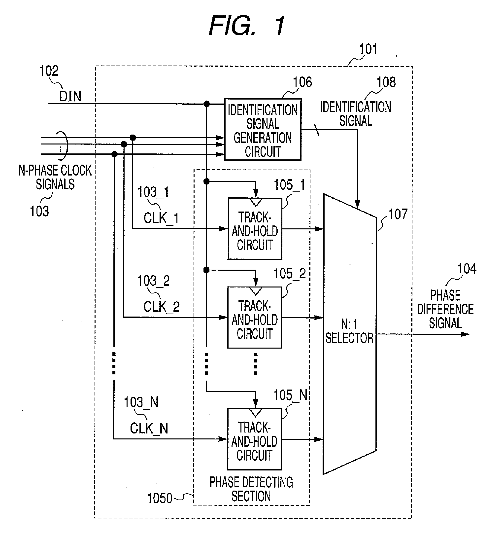
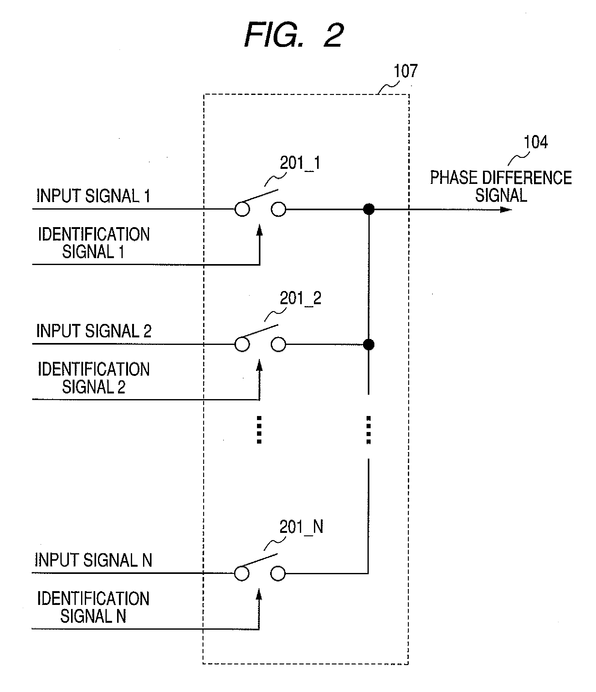
[0035]FIG. 1 is a block diagram of an example configuration of a phase detector circuit for a clock and data recovery circuit according to a first embodiment of the present invention. Referring to FIG. 1, a phase detector circuit 101 includes a phase detecting section 1050 having as many as N track-and-hold circuits 105_1 to 105_N (wherein N represents an integer of 2 or larger), an identification signal generation circuit 106, and an N:1 selector 107 used as a signal selection unit to select one out of as many as N signals. The track-and-hold circuits 105_1 to 105_N track, hold, and output, at a rising edge of an input data signal DIN (hereinafter also referred to simply as the “DIN”), N-phase clock signals 103 (i.e. 103_1 (CLK_1) to 103_N (CLK_N)) with phases shifted in 2π / N steps. The identification signal generation circuit 106 operating every time the DIN rises from low (L) to high (H) determines which one of the N-phase clock signals (CLK_1 to CLK_N) is closest in phase to 0 o...

second embodiment

[0047]FIG. 6 is a block diagram of an example configuration of a phase detector circuit for a clock and data recovery circuit according to a second embodiment of the present invention. The phase detector circuit shown in FIG. 6 includes a phase detecting section 2050 which has as many as N variable slew-rate driver circuits 604_1 to 604_N (wherein N represents an integer of 2 or larger), N tracking control switches 605_1 to 605_N, N tracked voltage holding capacitors 606_1 to 606_N, and N fixed-gain amplifiers 607_1 to 607_N, a logic inversion circuit 601, a DIN pulse selector circuit 602 for outputting DIN pulse selection signals 608 (SEL_1 to SEL_N), which are DIN pulse identification signals, a phase difference signal voltage holding capacitor 603, and holding control switches 608_1 to 608_N used as signal selection units. The phase detector circuit configured as described above is compatible with a 1 / N rate architecture, and the holding control switches, which are fundamental co...

third embodiment

[0071]FIG. 14 is a block diagram of an example configuration of an optical communication device 1400 according to a third embodiment of the present invention. The device complies with, for example, GPON, 10 GPON, or 100 G Ethernet (IEEE 802.3ba) and includes a phase detector circuit according to the first or the second embodiment of the present invention.

[0072]The optical communication device 1404 shown in FIG. 14 includes a digital logic circuit (higher-layer logic 1404) of layer 2 or higher, for example, a media access control (MAC) layer, a serializer / deserializer 1403 which performs conversion between a relatively low-speed, higher-layer digital signal and a high-speed serial signal (analog waveform), and an optical front-end section 1402 which performs conversion between an electrical signal inputted / outputted by the serializer / deserializer 1403 and an optical signal transmitted over an optical fiber.

[0073]An optical signal 1401 inputted from an optical fiber to the optical com...


PUM


Abstract

A high-accuracy phase detector circuit compatible with a 1 / N rate architecture is provided. The phase detector circuit has as many as N track-and-hold circuits for tracking and holding N-phase clock signals CLK—1 to CLK_N in synchronization with a rising edge of input data signal DIN. Out of the N-phase clock signals CLK—1 to CLK_N outputted from as many track-and-hold circuits, only the one whose rising edge is most synchronized with a rising edge of the input data signal DIN is selected and outputted as a phase difference signal.

Description

CLAIM OF PRIORITY[0001]The present application claims priority from Japanese patent application JP 2008-220787 filed on Aug. 29, 2008, the content of which is hereby incorporated by reference into this application.FIELD OF THE INVENTION[0002]The present invention relates to a phase detector circuit, particularly, to technology useful for application to a phase detector included in a clock and data recovery (CDR) circuit.BACKGROUND OF THE INVENTION[0003]In recent years, the bandwidth required for inter-chip data transmission has been rapidly expanding. To cope with the situation, serial transmission systems which are not affected by skews between signal lines have come to be widely used instead of parallel transmission systems which have been in use to transmit plural pieces of data and clock signals concurrently. In a serial transmission system, data with embedded clock signals is transmitted via a single signal line to be recovered into the data and clock signals by a CDR circuit o...

Claims


Application Information

Patent Timeline
Patent Type & Authority Applications(United States)
IPC IPC(8): H04B10/06H03D13/00H03K5/26H03L7/091H04L7/02
CPCH03D13/003H03L7/0807H04L7/0337H03L7/091H04B10/69H03L7/087
Inventor FUKUDA, KOJI
Owner HITACHI LTD
Why Eureka
Try Eureka