Activated gas injector, film deposition apparatus, and film deposition method
a technology of active gas and injector, which is applied in the direction of plasma technique, discharge tube/lamp details, coatings, etc., can solve the problems of poor uniformity of film properties and easy loss of active gas chemical activity, and achieve the effect of reducing thermal energy applied, easy loss of chemical activity, and high reactivity
Active Publication Date: 2010-03-04
TOKYO ELECTRON LTD
View PDF102 Cites 113 Cited by
- Summary
- Abstract
- Description
- Claims
- Application Information
AI Technical Summary
Benefits of technology
The patent text describes a method for deposition of high-dielectric films, such as silicon nitride or silicon oxide, using a plasma-based chemical vapor deposition method. The technical effects of the patent text include improved film quality with reduced thermal energy applied to the wafer, improved uniformity of film properties, and better impurity elimination. The patent also describes a film deposition apparatus that includes a plasma generation portion and a reaction gas nozzle to improve the concentration of activated reaction gas. Additionally, the patent describes a process apparatus for exposing a wafer to plasma to modify the properties of the deposited film. The technical effects of the patent text include improved film quality, reduced impurities, and better impurity elimination.
Problems solved by technology
This is because the activated gas can easily lose its chemical activity.
Method used
View moreImage
Smart ImageViewing Examples

Examples
example 1
[0215]The gas flow pattern in the injector body 321 of the activated gas injector 32 according to the first embodiment is first simulated.
example 2-1
[0222]Electrical power supplied to the heater 300 is adjusted so that a temperature measured by the temperature sensing terminal 305 is about 300° C.
example 2-2
[0223]Electrical power supplied to the heater 300 is adjusted so that a temperature measured by the temperature sensing terminal 305 is about 400° C.
Login to View More PUM
| Property | Measurement | Unit |
|---|---|---|
| temperatures | aaaaa | aaaaa |
| temperatures | aaaaa | aaaaa |
| diameter | aaaaa | aaaaa |
Abstract
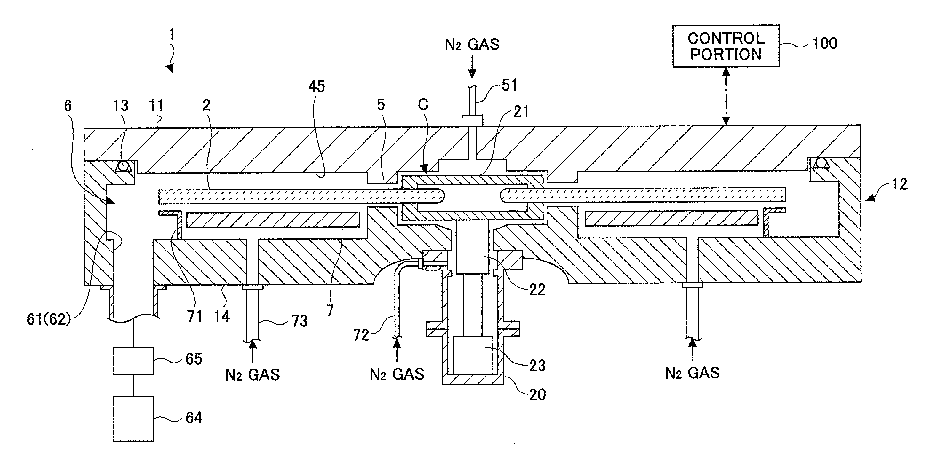
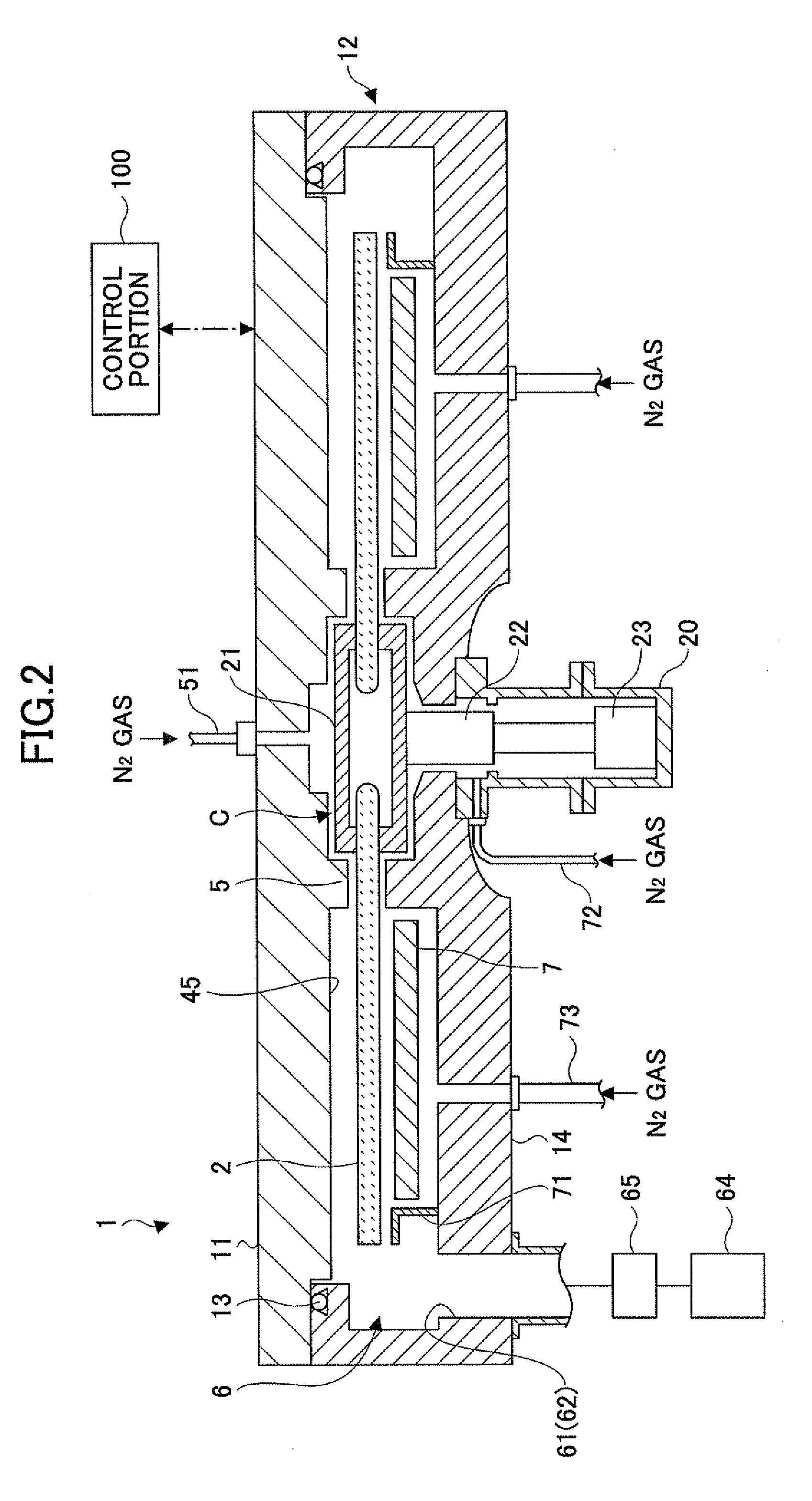
An activated gas injector includes a flow passage defining member partitioned into a gas activation passage and a gas introduction passage by a partition wall; a gas introduction port through which a process gas is introduced into the gas introduction passage; a pair of electrodes to be supplied with electrical power to activate the process gas, wherein the electrodes extend along the partition wall in the gas activation passage; through-holes formed in the partition wall and arranged along a longitudinal direction of the electrodes, wherein the through-holes allow the process gas to flow from the gas introduction passage to the gas activation passage; and gas ejection holes provided in the gas activation passage along the longitudinal direction of the electrodes, wherein the gas ejection holes allow the process gas activated in the gas activation passage to be ejected therefrom.
Description
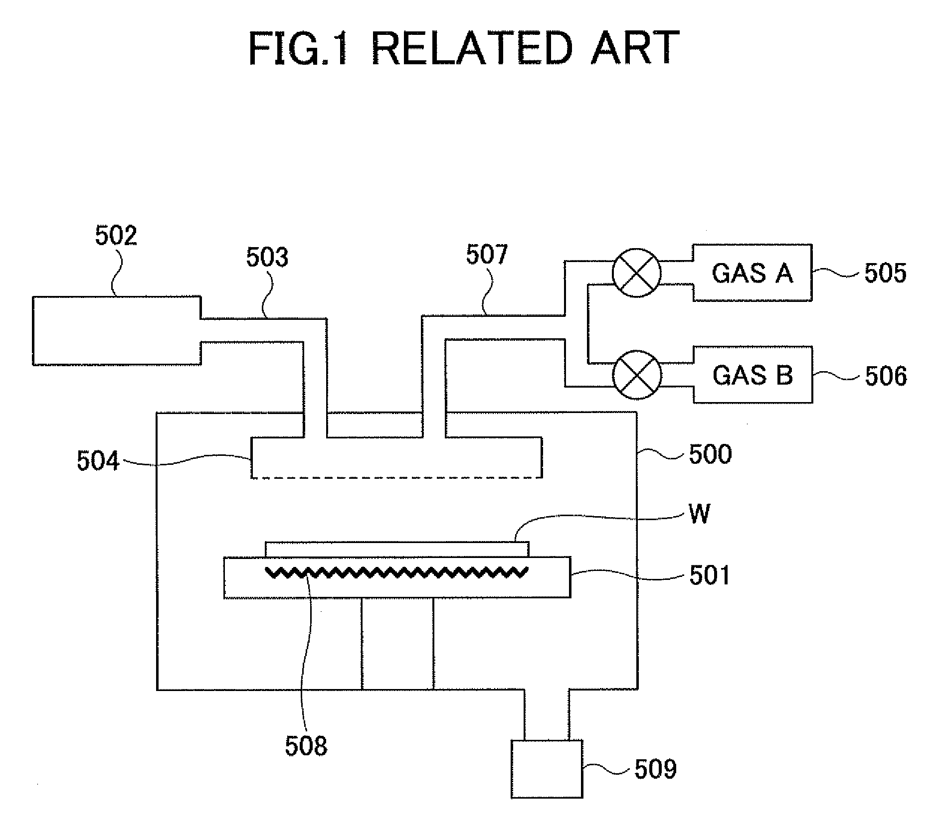
CROSS-REFERENCE TO RELATED APPLICATIONS[0001]The present application is based on Japanese Patent Applications No. 2008-222740, 2009-061605, and 2009-172948 filed with the Japanese Patent Office on Aug. 29, 2008, Mar. 13, 2009, and Jul. 24, 2009, respectively, the entire contents of which are hereby incorporated herein by reference.BACKGROUND OF THE INVENTION[0002]1. Field of the Invention[0003]The present invention relates to a technology for depositing a film on a substrate by carrying out plural cycles of supplying in turn at least two source gases to the substrate in order to form plural layers of a reaction product.[0004]2. Description of the Related Art[0005]As a film deposition technique in a semiconductor fabrication process, there has been known a process, in which a first reaction gas is adsorbed on a surface of a semiconductor wafer (referred to as a wafer hereinafter) and the like under vacuum and then a second reaction gas is adsorbed on the surface of the wafer in order...
Claims
Login to View More Application Information
Patent Timeline
 Patent Type & Authority Applications(United States)
IPC IPC(8): C23C16/50H05H1/24C23C16/00
CPCC23C16/452C23C16/45536C23C16/45551H01J37/32559H01J37/3244H01J37/32449C23C16/4584C23C16/45574C23C16/45517C23C16/45563C23C16/45565C23C16/45578C23C16/50C23C16/505C23C16/509C23C16/5093H01J1/00
Inventor KATO, HITOSHITAKEUCHI, YASUSHIUSHIKUBO, SHIGEHIROKIKUCHI, HIROYUKI
Owner TOKYO ELECTRON LTD
Features
- R&D
- Intellectual Property
- Life Sciences
- Materials
- Tech Scout
- Unparalleled Data Quality
- Higher Quality Content
- 60% Fewer Hallucinations
Learn More Browse by: Latest US Patents, China's latest patents, Technical Efficacy Thesaurus, Application Domain, Technology Topic, Popular Technical Reports.
© 2025 PatSnap. All rights reserved.Legal|Privacy policy|Modern Slavery Act Transparency Statement|Sitemap|About US| Contact US: help@patsnap.com