

Optical-semiconductor device and method for manufactruing the same
a technology of optical-semiconductor and manufacturing method, which is applied in the direction of semiconductor/solid-state device manufacturing, semiconductor devices, and surface-mounted optical-semiconductor devices. it can solve the problems of difficult formation of pits, difficult to produce thin optical-semiconductor devices, and difficult to make pits. small, to achieve the effect of improving light-extraction efficiency, easy production of thin optical-semiconductor devices, and high yield
- Summary
- Abstract
- Description
- Claims
- Application Information
AI Technical Summary
Benefits of technology
Problems solved by technology
Method used
Image

Examples
embodiment 1
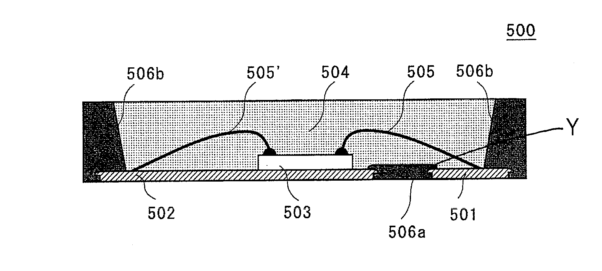
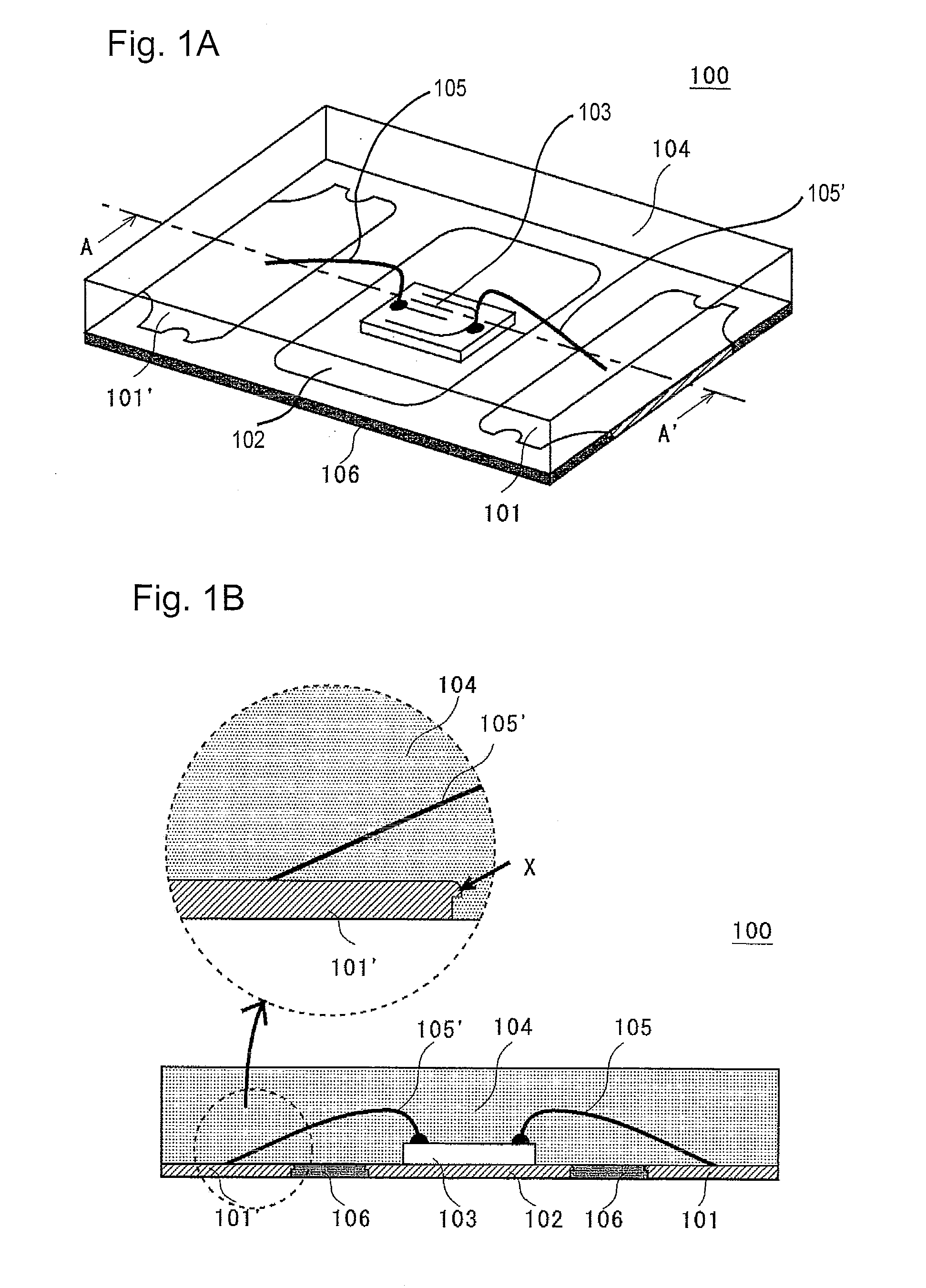
[0026]An optical-semiconductor device (light emitting device) 100 of this embodiment is shown in FIG. 1A and FIG. 1B. FIG. 1A is a perspective view of the light emitting device 100. FIG. 1B is a sectional view taken along lines A-A′ of the light emitting device 100 shown in FIG. 1A.
[0027]In this embodiment, the light emitting device 100 comprises a light emitting element 103, first electrically conductive members 101, 101′ that are electrically connected to the light emitting element 103, a second electrically conductive member 102 that is disposed separately from the first electrically conductive members 101, 101′ and has the light emitting element 103 mounted thereon, and a sealing member 104 that covers the light emitting element 103 and makes contact with the first electrically conductive members 101, 101′ and the second electrically conductive member 102 as shown in FIG. 1A and FIG. 1B. In addition, a base member 106 formed from a resin capable of blocking the light emitted by ...
embodiment 2
[0087]An optical-semiconductor device (light emitting device) 200 according to the second embodiment is shown in FIG. 3A and FIG. 3B. FIG. 3A is a perspective view showing the inside of the light emitting device 200 of the present invention, and FIG. 3B shows a sectional view taken along lines B-B′ of the light emitting device 200 shown in FIG. 3A with a recess thereof being sealed.
[0088]The light emitting device 200 of the second embodiment comprises (a) a light emitting element 203 and a protective element 210, (b) a first electrically conductive member 201 electrically connected to the light emitting element 203 and to the protective element 210, (c) a second electrically conductive member 202 that is disposed separately from the first electrically conductive member 201 and has the light emitting element 203 mounted thereon, and (d) a sealing member 204 that covers the light emitting element 203 and contacts with the first electrically conductive member 201 and with the second el...
embodiment 3
[0097]FIG. 5 is a perspective view showing the optical-semiconductor device of the present invention, with a part thereof being cut away to reveal the inside of a base member 306. In the third embodiment, a light emitting element 303 is mounted in a recess S2 that is surrounded by the protruding portion 306 of the base member, and a protective element 310 is embedded in the protruding portion 306 of the base member, as shown in FIG. 5. FIG. 5 is a diagram showing the inside of a part of the base member 306 of the optical-semiconductor device that has substantially rectangular parallelepiped shape as shown in FIG. 3A.
[0098]In the second step, before forming the base member, the protective element 310 is placed on the second electrically conductive member 302 and is connected to the first electrically conductive member 301 by means of the electrically conductive wire 305. Thus such a structure can be made as the protective element 310 is embedded in the base member 306. In the first e...
PUM
 Abstract
Description
Claims
Application Information