Semiconductor device and manufacturing method for the same

a technology of semiconductor devices and manufacturing methods, applied in the direction of semiconductor devices, basic electric elements, electrical appliances, etc., can solve the problems of no established system and system for obtaining appropriate terminal parts, and achieve the effect of increasing breakdown voltage, high stable breakdown voltage, and simplifying the process design of super junction structures

Inactive Publication Date: 2010-03-11
SONY CORP
View PDF2 Cites 39 Cited by
  • Summary
  • Abstract
  • Description
  • Claims
  • Application Information

AI Technical Summary

Benefits of technology

[0034]In each of the second and third embodiment, the semiconductor device is also formed by a simple process in which both an element part and a terminal part around the element part are provided with super junction structures. Although it is not more than the first embodiment, in the semiconductor device, the presence of a lateral RESURF region that functions as an extended depletion layer region on the terminal part allows a region to be depleted at the time of applying a drain voltage (in the off state) to be extended to the terminal part. Therefore, the resulting semiconductor device is free of concentrated electric field. In addition, an increase in breakdown voltage is attained while the impurity concentration of the second semiconductor region on the terminal part is kept high. Furthermore, the impurity concentration of a first pillar region of the element part is substantially equal to the impurity concentration of a first pillar region of the terminal part. Thus, the process design of a super junction structure can be simplified.
[0035]According to any embodiment of the present invention, the semiconductor device is formed by a simple process in which both an element part and a terminal part around the element part are provided with super junction structures. Since the lateral RESURF region exists in the terminal part, a high stable breakdown voltage is realizable.

Problems solved by technology

However, the third manufacturing method have problems in conditions for preventing the generation of any defect during epitaxial growth to a trench groove and control of the amount of impurities to be doped.
Actually, any system for obtaining an appropriate terminal part has not been established in the formation of the super junction structure by the third manufacturing method.
Although the relative arrangement of the trench groove of the element part and the trench groove of the terminal groove may be sufficiently considered, there is no established system for such an arrangement.

Method used


Image

  • Semiconductor device and manufacturing method for the same
  • Semiconductor device and manufacturing method for the same
  • Semiconductor device and manufacturing method for the same

Examples


first embodiment

on

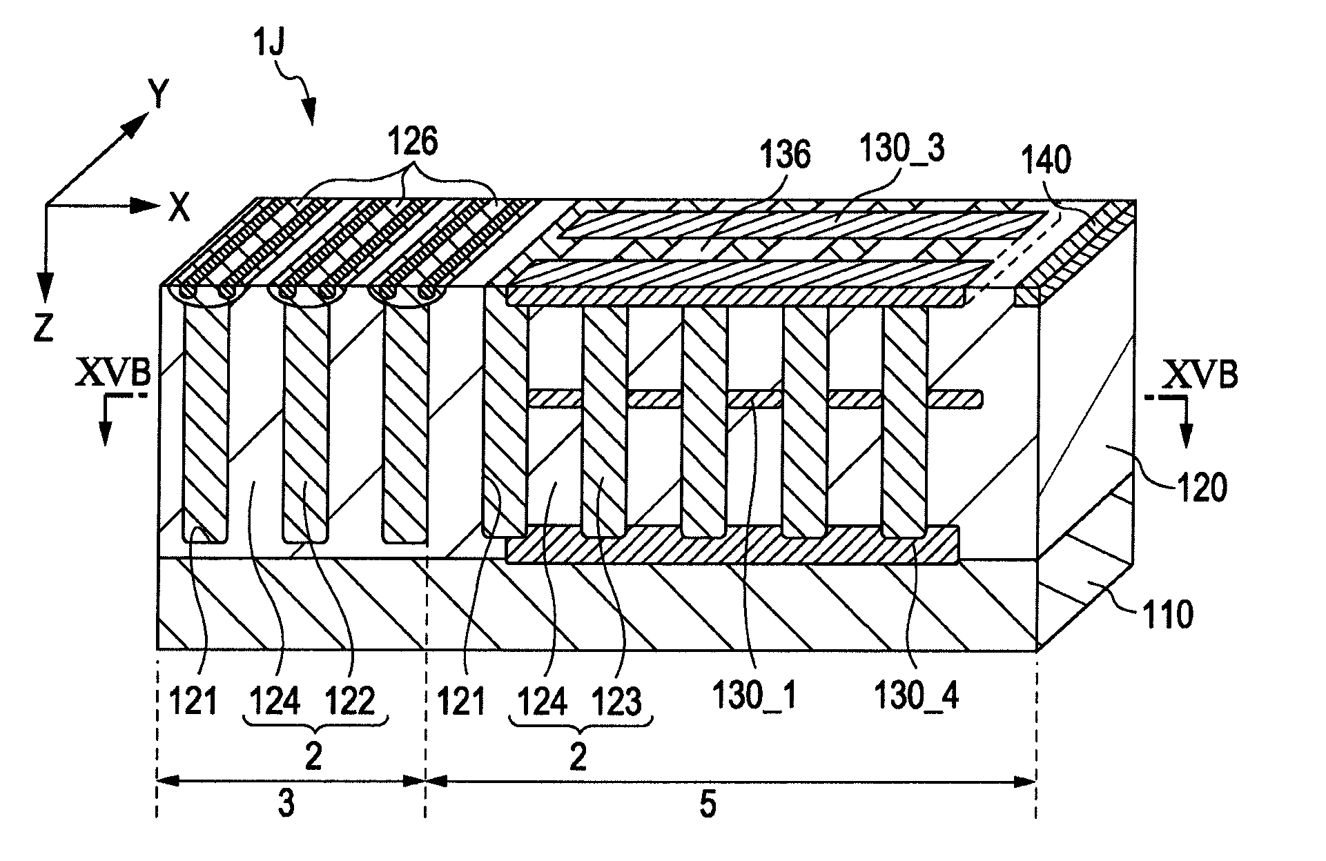
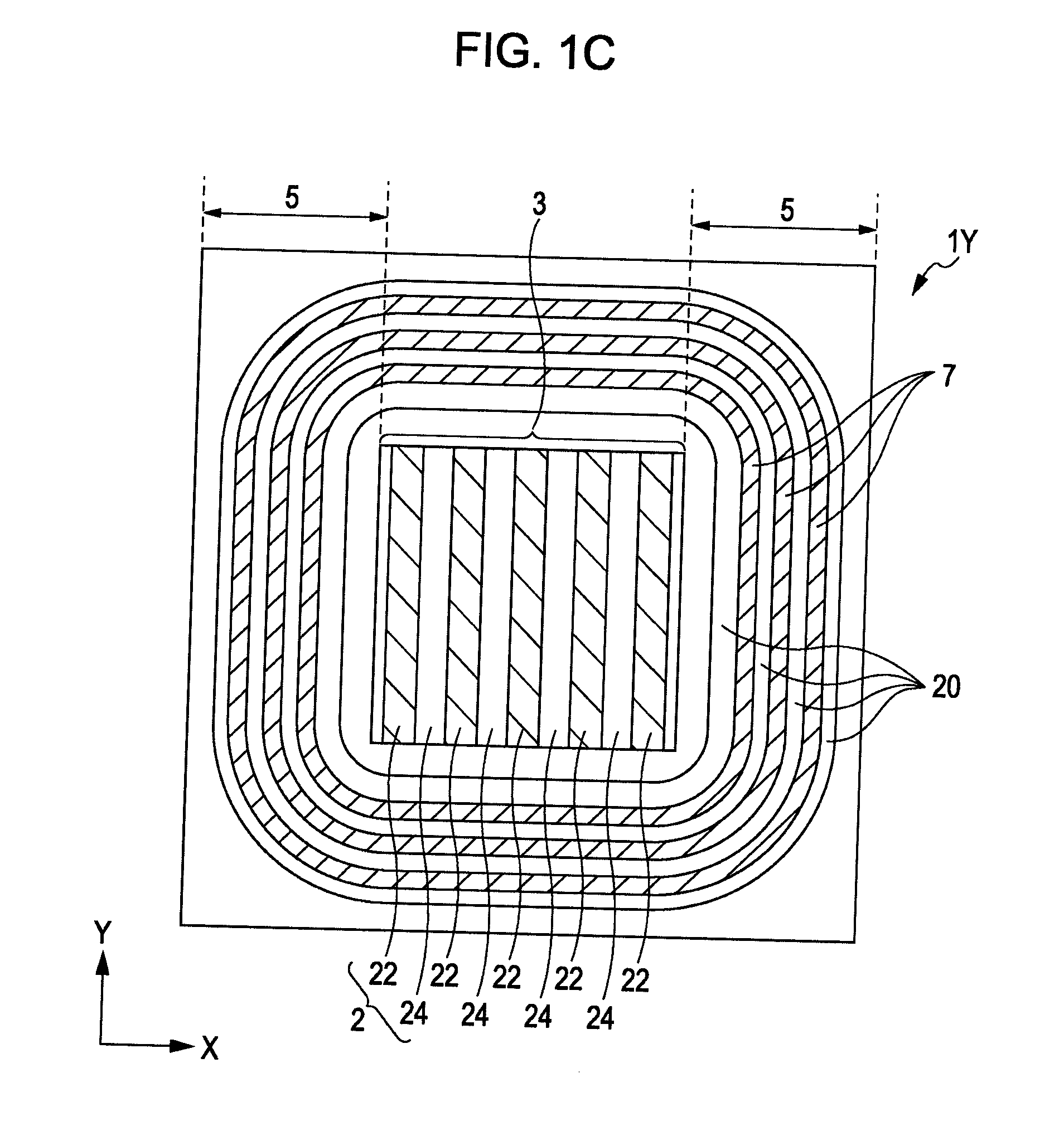
[0106]FIG. 2A to FIG. 2E illustrate the configuration of a semiconductor device 1A_1 according to a first embodiment (basic configuration) of the present invention. Here, FIG. 2A is a perspective diagram schematically illustrating the configuration of almost the half part of the semiconductor device 1A_1. FIG. 2B and FIG. 2C are schematic diagrams illustrating the configuration of the boundary between an element part 3 and a terminal part 5 of the semiconductor device 1A_1, where FIG. 2B is a schematic perspective view of the semiconductor device 1A_1 and FIG. 2C is a cross-sectional view of the semiconductor device 1A_1 along the IIC-IIC line in X-Y directions in FIG. 2B. FIG. 2D is a plan view (transparent view) of the semiconductor device 1A_1 with reference to the X-Y plane in FIG. 2B and the X-Y plane in FIG. 2C. In this figure, a source region is omitted, while both a base region and a gate electrode are illustrated. Any of these diagrams is only provided for diagrammatic il...

first modified example

Manufacturing Method: First Embodiment: First Modified Example

[0159]FIG. 5A and FIG. 5B illustrate an exemplary process for manufacturing the semiconductor device 1A_2 having the basic configuration according to the first embodiment (first modified example). The following description will focus on the difference with the manufacturing method of the semiconductor device 1A_1 according to the first embodiment (basic configuration).

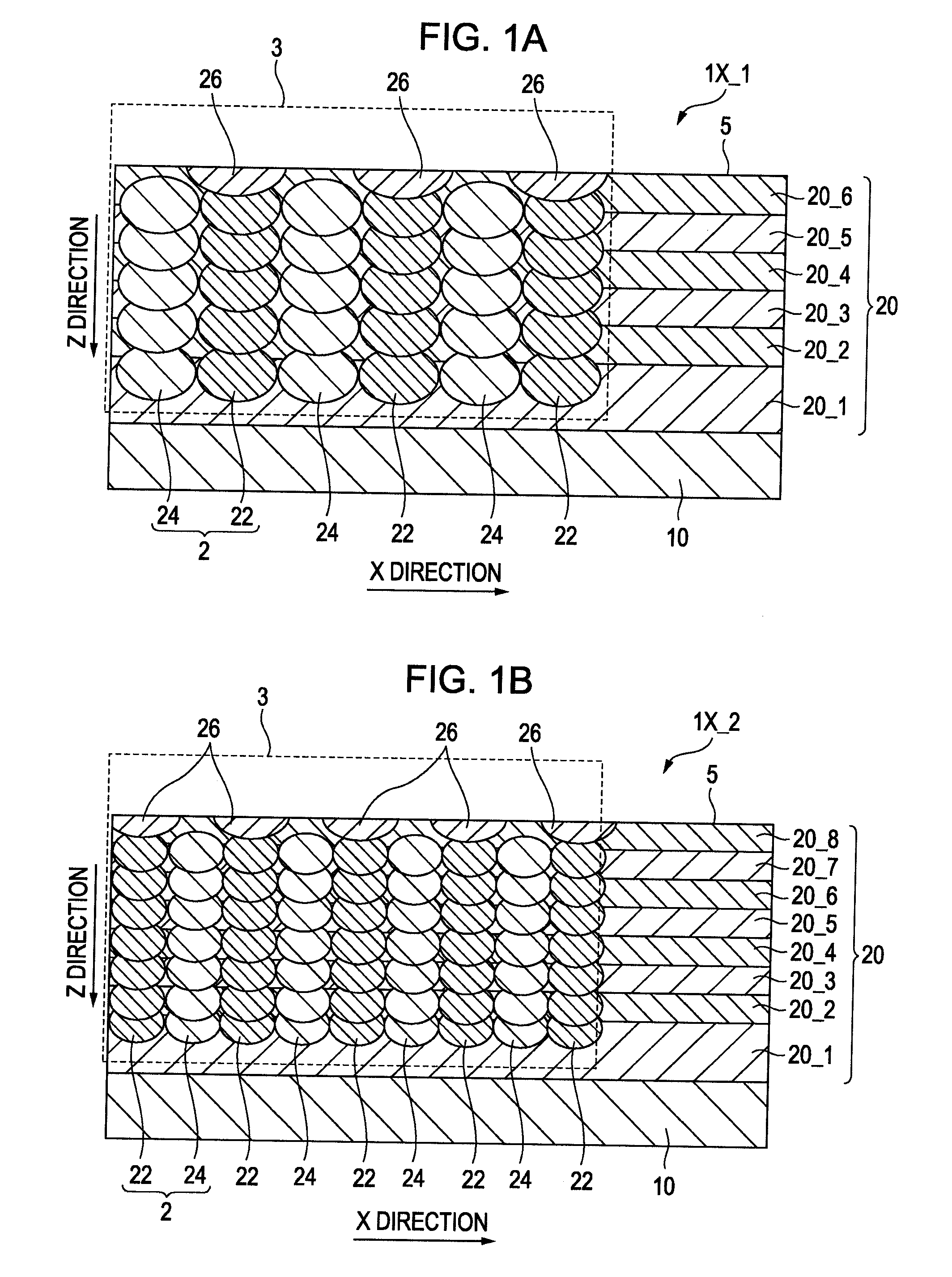
[0160]A trench-formation epitaxial-refilling method (the third manufacturing method) is applied to the formation of p-type epitaxial buried layers 122 and 123. At this time, however, the process may be performed in consideration of forming a p-type lateral RESURF region 130 on the middle portion of the n-type epitaxial layer 120 in the terminal part 5 to prevent from overlapping with the p-type epitaxial buried layer 123. For example, the process includes the steps of forming a first n-type epitaxial layer 120_1, forming a p-type lateral RESURF region 130, f...

second modified example

Manufacturing Method: First Embodiment: Second Modified Example

[0173]FIG. 7 illustrates an exemplary process for manufacturing the semiconductor device 1A_3 having the basic configuration according to the first embodiment (second modified example). The following description will focus on the difference with the manufacturing method of the semiconductor device 1A_2 according to the first embodiment (second modified example).

[0174]In principle, like the first embodiment (first modified example), the formation of trench grooves and the embedding growth may be carried out only once. At this time, however, the process may be performed in consideration of patterning an opening 132 to prevent the generation of overlap with the p-type epitaxial buried layer 123 at the time of forming the p-type lateral RESURF region 130 on the middle portion of the n-type epitaxial layer 120 in the terminal part 5.

[0175]First, an n-type epitaxial layer 120_1 is formed up to one half of the desired film thic...


PUM


Abstract

A semiconductor device includes a first conductive type first semiconductor region, a second semiconductor region, and a second conductive type lateral RESURF region. The first semiconductor region is arranged on a first electrode side. The second semiconductor region includes first conductive type first pillar regions and a terminal part. The second pillar regions are alternately arranged on an element part. The terminal part is formed around the element part along a surface of the first semiconductor region on a second electrode side opposite to the first electrode side of the first semiconductor region. Furthermore, the second conductive type lateral RESURF region is formed in the second semiconductor region on the terminal part.

Description

BACKGROUND OF THE INVENTION[0001]1. Field of the Invention[0002]The present invention relates to a semiconductor device and a manufacturing method of the same. More specifically, the present invention relates to a semiconductor device with a super junction structure and a manufacturing method of the same.[0003]2. Description of the Related Art[0004]In recent years, there are increasing demands for thin-shaped, lightweight electronic apparatuses represented by a liquid crystal TV, a plasma TV, and an organic EL TV. In connection with such demands, there are other strong demands for small-sized high-performance power supply devices. In response to such demands, for example, efforts have been made to improve the performance of a power semiconductor, such as improvements in properties of withstand voltage (breakdown voltage), high current, low loss, high speed, and high breakdown voltage. For example, a power MOSFET has been known as a switching element for power electronics.[0005]The o...

Claims


Application Information

Patent Timeline
Patent Type & Authority Applications(United States)
IPC IPC(8): H01L29/78H01L21/768
CPCH01L29/0619H01L29/063H01L29/0634H01L29/7811H01L29/1095H01L29/66712H01L29/0696
Inventor SASAKI, YUJI
Owner SONY CORP
Why Eureka
Try Eureka