Gated resonant tunneling diode

a tunneling diode and resonant technology, applied in the direction of diodes, semiconductor devices, electrical apparatus, etc., can solve the problems of not having the desired properties of a transistor, rtds can be manufactured with conventional cmos technology, and short of providing a next-generation, manufacturable transistor

Active Publication Date: 2010-03-18
TEXAS INSTR INC
View PDF2 Cites 8 Cited by
  • Summary
  • Abstract
  • Description
  • Claims
  • Application Information

AI Technical Summary

Problems solved by technology

However, each falls short of providing a next-generation, manufacturable transistor.
RTDs can be manufactured with conventional CMOS technology, but do not have the desired properties of a transistor, and known quantum mechanical transistors usually require special (and prohibitively expensive) manufacturing and / or operate under cryogenic conditions (i.e., require liquid nitrogen cooling).

Method used


Image

  • Gated resonant tunneling diode
  • Gated resonant tunneling diode
  • Gated resonant tunneling diode

Examples


Embodiment Construction

[0039]Refer now to the drawings wherein depicted elements are, for the sake of clarity, not necessarily shown to scale and wherein like or similar elements are designated by the same reference numeral through the several views.

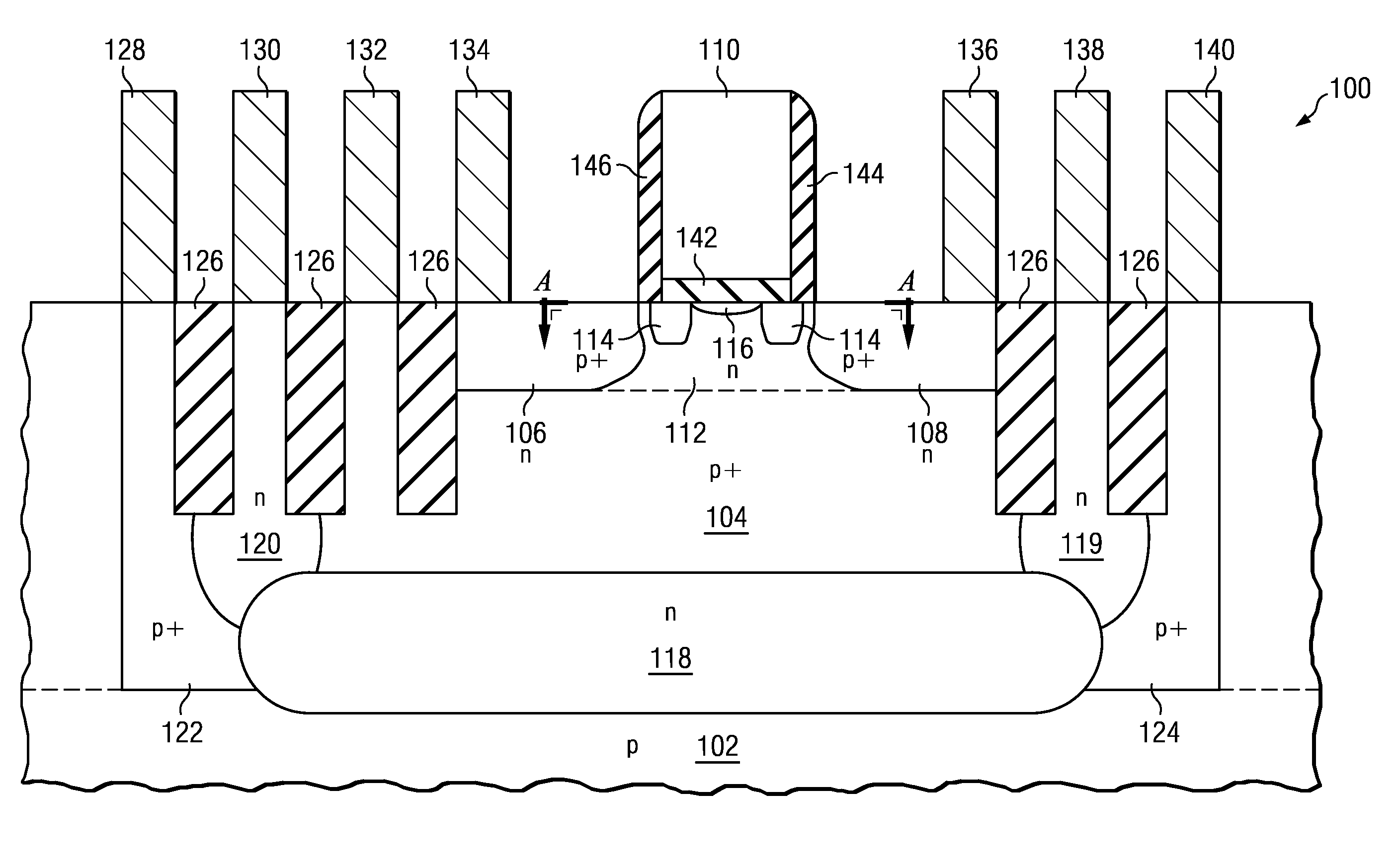
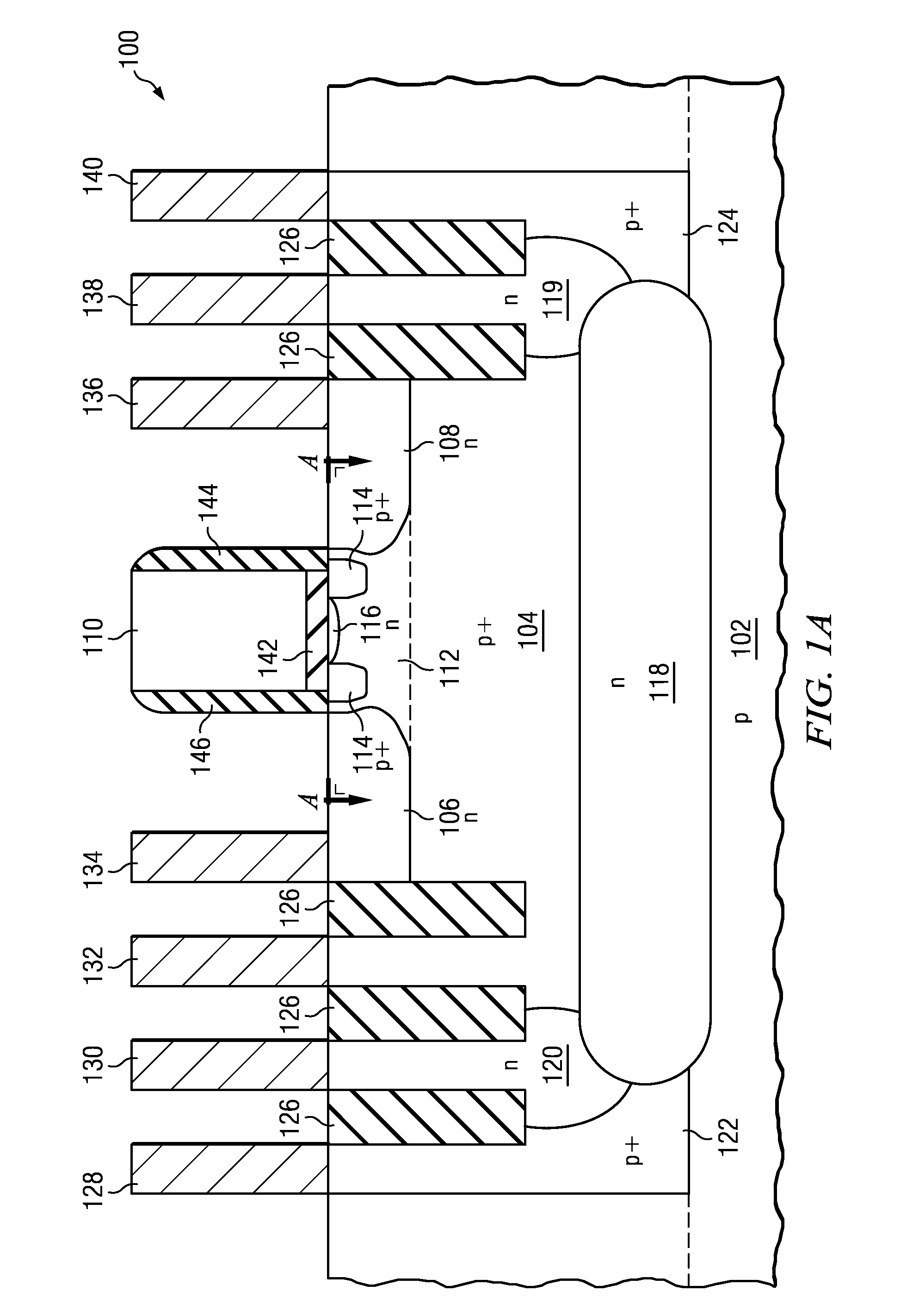
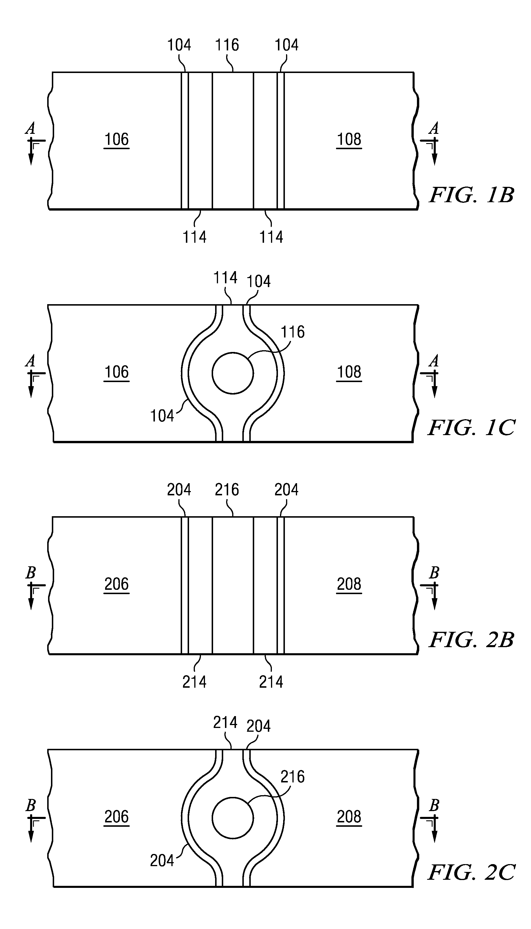
[0040]Referring to FIGS. 1A-1C of the drawings, the reference numeral 100 generally designates an NMOS gated resonant tunneling diode (GRTD) in accordance with a preferred embodiment of the present invention. GRTD 100 generally comprises a substrate 102, a body 104, an electrode region or source 106, an electrode region or drain 108, channel or channel region 112, barrier region 114, quantum well region 116, deep N-well or DNWell 118, shallow N-wells or NWells 119 and 120, shallow P-wells or PWells 122 and 124, shallow trench isolation (STI) 126, contacts 128, 130, 132, 134, 136, 138, and 140, insulating or gate oxide layer 142, control or gate electrode 110, and insulating layers 144 and 146.

[0041]Preferably, GRTD 100 is formed using conventional CMOS process...


PUM


Abstract

A gated resonant tunneling diode (GRTD) that operates without cryogenic cooling is provided. This GRTD employs conventional CMOS process technology, preferably at the 65 nm node and smaller, which is different from other conventional quantum transistors that require other, completely different process technologies and operating conditions. To accomplish this, the GRTD uses a body of a first conduction type with a first electrode region and a second electrode region (each of a second conduction type) formed in the body. A channel is located between the first and second electrode regions in the body. A barrier region of the first conduction type is formed in the channel (with the doping level of the barrier region being greater than the doping level of the body), and a quantum well region of the second conduction type formed in the channel. Additionally, the barrier region is located between each of the first and second electrode regions and the quantum well region. An insulating layer is formed on the body with the insulating layer extending over the quantum well region and at least a portion of the barrier region, and a control electrode region is formed on the insulating layer.

Description

CROSS-REFERENCE TO RELATED APPLICATIONS[0001]This application is a continuation-in-part of U.S. patent application Ser. No. 12 / 204,604, entitled “GATED QUANTUM RESONANT TUNNELING DIODE USING CMOS TRANSISTOR WITH MODIFIED POCKET AND LDD IMPLANTS,” filed on Sep. 4, 2008, which is a nonprovisional application of U.S. Provisional Application No. 60 / 969,772, filed Sep. 4, 2007, the entireties which are hereby incorporated by reference for all purposes.TECHNICAL FIELD[0002]The invention relates generally to quantum mechanical transistor and, more particularly, to a gated resonant tunneling diode (GRTD).BACKGROUND[0003]Resonant tunneling diodes (RTDs) have been used for many years and have been extensively studied. Additionally, quantum mechanical transistors have been the focus of study for many years as well. However, each falls short of providing a next-generation, manufacturable transistor. RTDs can be manufactured with conventional CMOS technology, but do not have the desired properti...

Claims


Application Information

Patent Timeline
Patent Type & Authority Applications(United States)
IPC IPC(8): H01L29/88H01L29/78
CPCH01L27/0629H01L27/0811H01L29/882H01L29/66931H01L29/107
Inventor EDWARDS, HENRY L.BOWEN, ROBERT C.CHATTERJEE, TATHAGATA
Owner TEXAS INSTR INC
Why Eureka
Try Eureka