Liquid crystal device and electronic apparatus

a liquid crystal device and electronic equipment technology, applied in non-linear optics, instruments, optics, etc., can solve the problems of reducing the transmittance, wavelength dependence of birefringent index, and dispersing of liquid crystal layer (liquid crystal material)

Active Publication Date: 2010-03-18
138 EAST LCD ADVANCEMENTS LTD
View PDF5 Cites 55 Cited by
  • Summary
  • Abstract
  • Description
  • Claims
  • Application Information

AI Technical Summary

Benefits of technology

[0008]An advantage of some aspects of the invention is to solve at least some of the above pro...

Problems solved by technology

One of the problems of such a transverse electric field mode liquid crystal device is wavelength dispersion of the liquid crystal layer...

Method used


Image

  • Liquid crystal device and electronic apparatus
  • Liquid crystal device and electronic apparatus
  • Liquid crystal device and electronic apparatus

Examples


first embodiment

[0048]Hereinafter, a transmissive color liquid crystal device (hereinafter, it is referred to as a “liquid crystal device”) using a FFS mode according to a first embodiment will be described with reference to the accompanying drawings. Furthermore, in all the following drawings, since the size of each component is set to be recognizable on the drawings, the dimensions and proportions of each component are properly set to be different from actual dimensions and proportions.

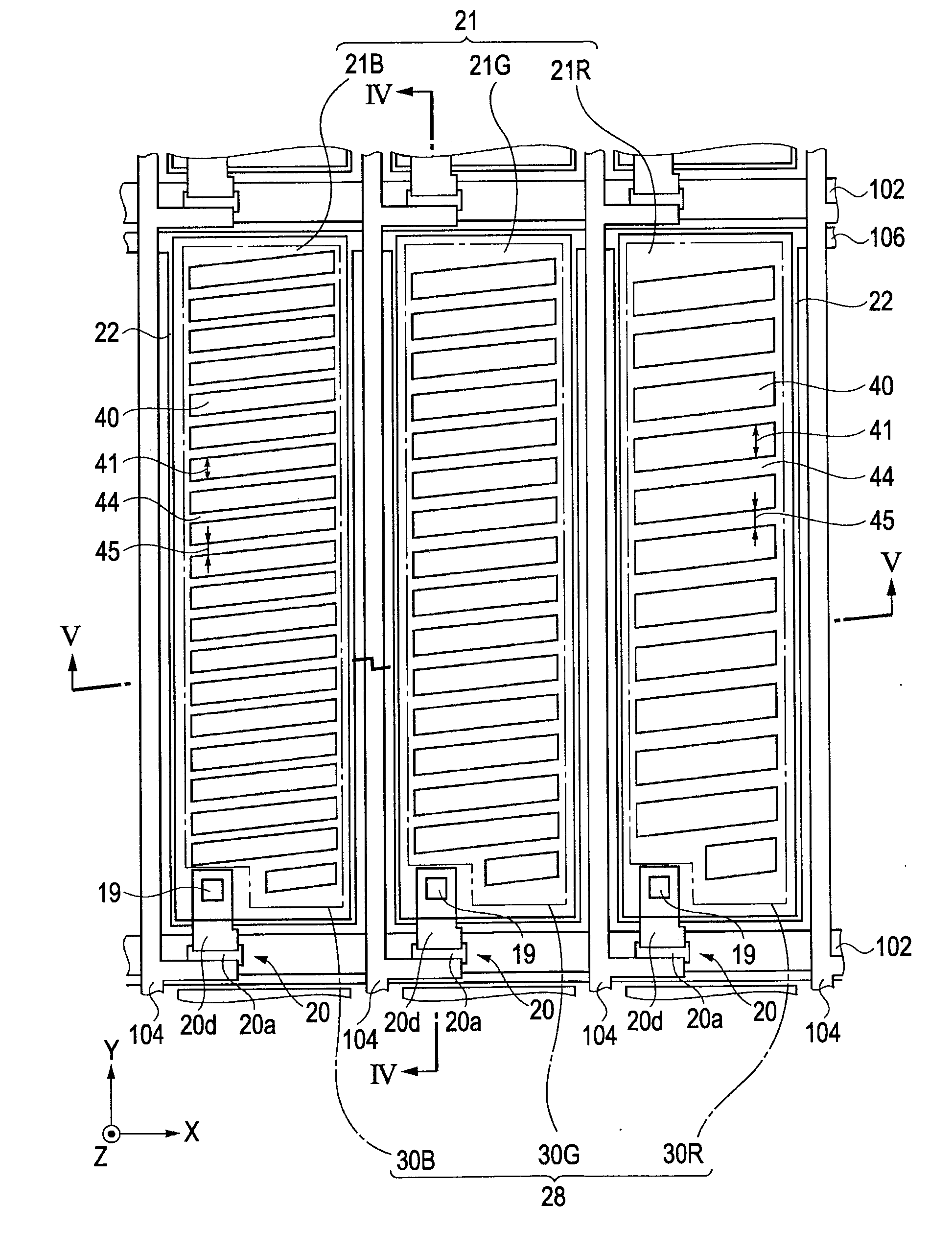
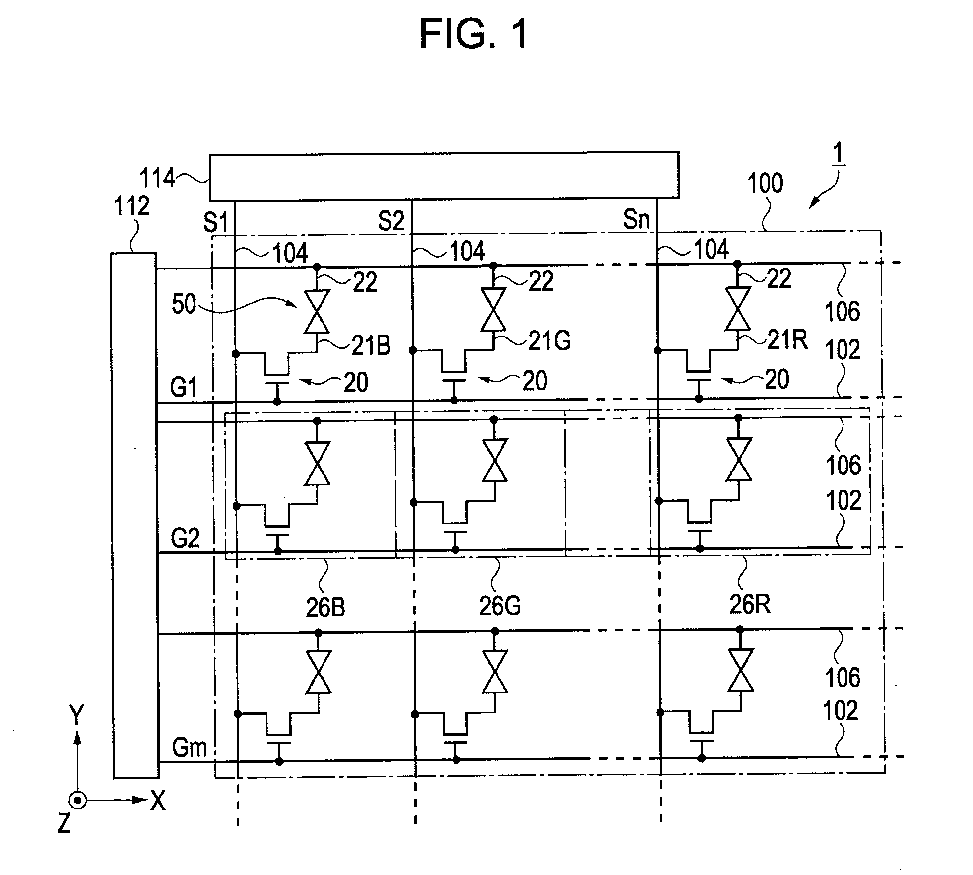
[0049]FIG. 1 is a circuit diagram of a liquid crystal device 1 according to the embodiment. Each of a plurality of sub-pixels 26 regularly arranged in a display region 100 of the liquid crystal device 1 is provided with a pixel electrode 21 as a first electrode capable of applying a voltage between itself and a common electrode 22 as a second electrode; and a TFT (thin film transistor) 20 for controlling switching of the pixel electrode 21. The common electrode 22 is electrically connected to common lines 106 exten...

second embodiment

[0097]Subsequently, a second embodiment of the invention will be described. FIG. 7 is a view schematically illustrating a section of the liquid crystal device 2 according to the second embodiment. FIG. 7 is a sectional view taken along the line which is the same as the section line of the sectional view of the liquid crystal device 1 according to the first embodiment shown in FIG. 5. The liquid crystal device 2 according to the present embodiment has a configuration similar to the liquid crystal device 1 according to the first embodiment. The components formed on the array substrate 10 are substantially the same except for the layer thickness of the interlayer insulation layer 51. The section taken along the line IV-IV of FIG. 3 is also substantially the same except for the existence of a liquid-crystal-thickness adjustment layer 57 to be described later. Therefore, the liquid crystal device 2 according to the embodiment will be described with reference to only FIG. 7 which is a sec...

third embodiment

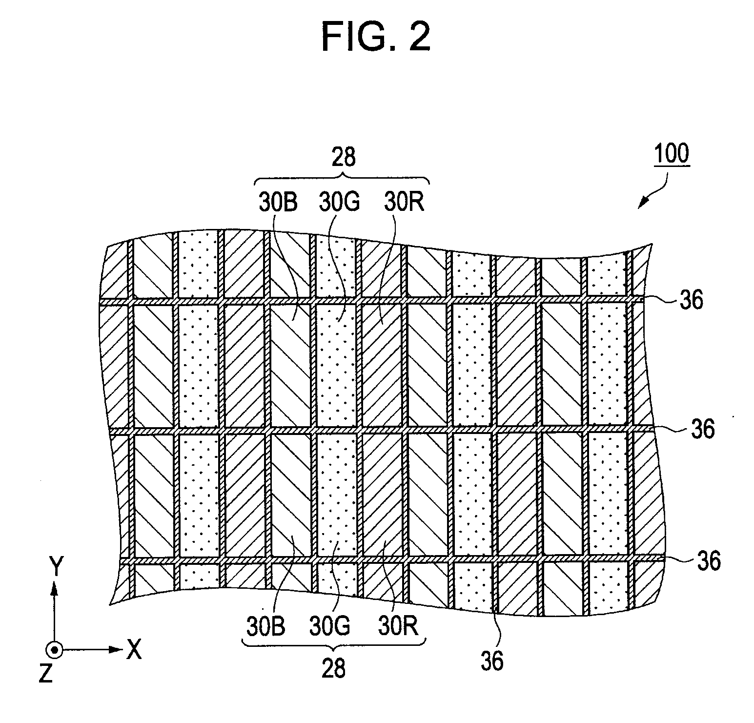
[0107]Subsequently, a third embodiment of the invention will be described. FIG. 9 is a view schematically illustrating a planar configuration of the pixel region 28 of the liquid crystal device 3 according to the third embodiment, where the pixel region 28 includes the blue sub-pixel region 30B, the green sub-pixel region 30G, and the red sub-pixel region 30R. In addition, FIG. 9 corresponds to FIG. 3 in the above-mentioned first embodiment, and is a view of the array substrate 10 (refer to FIG. 10) viewed from the normal direction. Accordingly, the color filters 35 and the like formed on the counter substrate 11 (refer to FIG. 10) are not shown.

[0108]FIG. 10 is a sectional view taken along the line X-X shown in FIG. 9, and is a view corresponding to the sectional view of the liquid crystal device 1 according to the first embodiment shown in FIG. 5 and to the sectional view of the liquid crystal device 2 according to the second embodiment shown in FIG. 7.

[0109]In both drawings, when...


PUM


Abstract

A liquid crystal device includes: a liquid crystal layer which is sandwiched between a pair of substrates; a color filter layer has a first coloration layer for transmitting a first light and a second coloration layer for transmitting a second light; first electrodes has a first pixel electrode disposed on a first sub-pixel region corresponding to a planar region of the first coloration layer and a second pixel electrode disposed on a second sub-pixel region corresponding to a planar region of the second coloration layer; and second electrodes each of which faces each first electrode. Any one electrode of each first electrode and each second electrode has a plurality of band-like portions which are arranged at predetermined intervals. A layer thickness of the liquid crystal layer, a width of each band-like portion, and the predetermined intervals within the first sub-pixel region are smaller than they within the second sub-pixel region.

Description

BACKGROUND[0001]1. Technical Field[0002]The present invention relates to a liquid crystal device and an electronic apparatus.[0003]2. Related Art[0004]Examples of methods of achieving an increase in the angle of view of known liquid crystal devices include a mode (hereinafter, it is referred to as a transverse electric field mode) for controlling the alignment of liquid crystal molecules by applying an electric field along the surface of a substrate to a liquid crystal layer. For example, an FFS (Fringe-Field Switching) mode has been known as the transverse electric field mode (Japanese Patent No. 3498163). A liquid crystal device using such a transverse electric field mode is configured to generate a transverse electric field in a liquid crystal layer by applying a voltage between a pair of electrodes formed on one of a pair of substrates sandwiching the liquid crystal layer. By adopting such a configuration, liquid crystal molecules in the liquid crystal layer are rotated in a hor...

Claims


Application Information

Patent Timeline
IPC IPC(8): G02F1/1335G02F1/1343
CPCG02F1/133514G02F2001/134372G02F1/134363G02F1/134372G02F1/1343
Inventor TSUCHIYA, HITOSHIIKEBE, TOMOOKUMURA, OSAMU
Owner 138 EAST LCD ADVANCEMENTS LTD
Why Eureka
Try Eureka