Ceramic electronic component and method for manufacturing the same

a technology of ceramic electronic components and components, which is applied in the direction of fixed capacitor details, variable capacitors, fixed capacitors, etc., can solve the problems of cracks likely to develop at the portion of the ceramic component body, and cracks likely to develop in the ceramic component body

Active Publication Date: 2010-03-18
MURATA MFG CO LTD
View PDF6 Cites 33 Cited by
  • Summary
  • Abstract
  • Description
  • Claims
  • Application Information

AI Technical Summary

Benefits of technology

[0009]In view of the above, preferred embodiments of the present invention provide a ceramic electronic component that is hardly influenced by the stress generated when an external electrode containing a metal sintered compact is formed at the end of the ceramic component body, and a method for manufacturing the same.

Problems solved by technology

In the ceramic electronic component having the metal layer formed at the end surface of the ceramic electronic component body, a large stress is applied to the metal layer due to a thermal shock cycle in which increases and decreases in temperatures are repeated, sometimes resulting in development of cracks in the ceramic component body.
Since such a stress is concentrated on the end of the metal layer at the side surface of the ceramic component body, cracks are likely to develop at the portion in the ceramic component body.
Thus, cracks are likely to develop in the ceramic component body.
When the wiring board to which the ceramic electronic component is attached bends to apply a stress caused by the bending of the wiring board, cracks are likely to develop at the end of the metal layer in the ceramic component body.
Such cracks reach the internal electrodes, the properties of the ceramic electronic component are affected.

Method used


Image

  • Ceramic electronic component and method for manufacturing the same
  • Ceramic electronic component and method for manufacturing the same
  • Ceramic electronic component and method for manufacturing the same

Examples


example 1

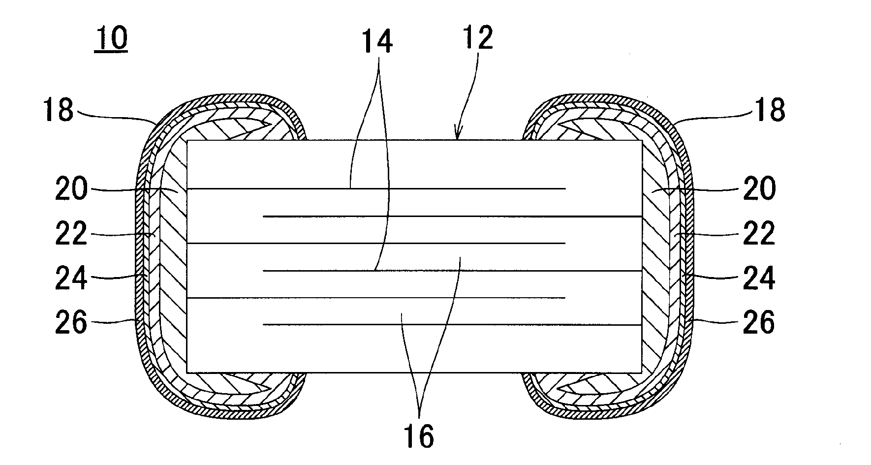
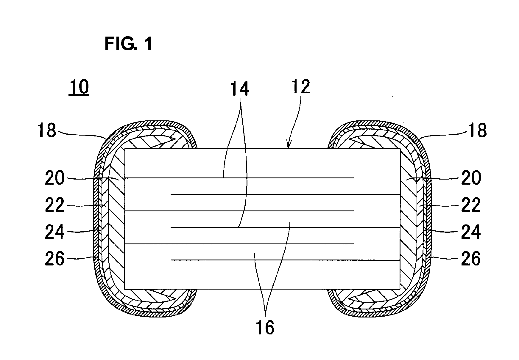
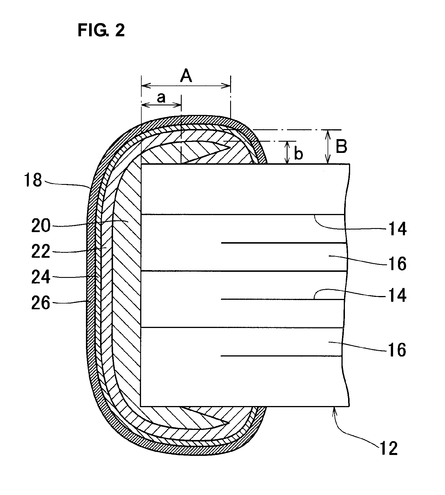
[0057]In order to manufacture a laminated ceramic capacitor, an about 1.0 mm×0.5 mm×0.5 mm fired ceramic chip and an about 3.2 mm×2.5 mm×2.5 mm fired ceramic chip were prepared as the ceramic component body 12. In the ceramic chip, internal electrode layers and ceramic layers were alternately laminated, and each of the internal electrodes is led to the facing end surface. On the ceramic chip, a metal electrode as the first external electrode 20 was formed. For the formation thereof, a conductive paste, in which Cu powder, glass frit, acryl, varnish, and a solvent were mixed and dispersed with a three-roll mill, was prepared. The end surface of the ceramic chip was immersed in the conductive paste, and fired to form a metal electrode. The firing was performed using a temperature profile in which the ceramic chip to which the conductive paste was applied was held at the maximum temperature of about 870° C. for about 5 minutes in a belt furnace.

[0058]For samples in which the end of the...


PUM

PropertyMeasurementUnit
temperatureaaaaaaaaaa
softening pointaaaaaaaaaa
shrinkageaaaaaaaaaa

Abstract

A ceramic electronic component that is hardly influenced by a stress generated when an external electrode containing a metal sintered compact is formed at the end of the ceramic component body, and a method for manufacturing the same are provided. A laminated ceramic capacitor includes a ceramic component body and first electrodes to be connected to internal electrodes that are led to the end surfaces are formed. The first external electrodes are arranged so that the ends are spaced apart from the side surfaces of the ceramic component body. Second external electrodes containing a conductive resin are arranged so as to entirely cover the first electrodes and first and second metal layers and are formed thereon. The first external electrodes are formed by supplying a conductive paste containing conductive metal powder and glass frit having a softening point higher than the sintering starting temperature of the conductive metal powder, and heating the same.

Description

BACKGROUND OF THE INVENTION[0001]1. Field of the Invention[0002]The present invention relates to a ceramic electronic component and a method for manufacturing the same. In particular, the present invention relates to a ceramic electronic component, such as a laminated ceramic capacitor, in which a terminal electrode is formed at the end surface of a ceramic component body and a method for manufacturing the same.[0003]2. Description of the Related Art[0004]FIG. 9 is a diagram illustrating an example of a conventional ceramic electronic component. A ceramic electronic component 1 contains a ceramic electronic component body 2. The ceramic electronic component body 2 contains layers of internal electrodes 3 and ceramic layers 4. The internal electrodes 3 are led to two end surfaces of the ceramic electronic component body 2. A metal layer 5 is formed in such a manner as to be connected to the internal electrodes 3. The metal layer 5 is formed by printing a conductive paste containing m...

Claims


Application Information

Patent Timeline
Patent Type & Authority Applications(United States)
IPC IPC(8): H01G4/232B05D5/12
CPCH01G4/228Y10T29/435H01G4/232H01G4/33H01G4/30
Inventor KOGA, SEIJI
Owner MURATA MFG CO LTD
Why Eureka
Try Eureka