

Adhesive tape and semiconductor device using the same
a technology of adhesive tape and semiconductor chip, which is applied in the direction of solid-state devices, electrical devices, synthetic resin layered products, etc., can solve the problems of difficult to ensure the reliability of electrical connection between semiconductor chips and resin ion migration after filling, and achieve the improvement of electrical connection reliability between semiconductor chips, good ion migration resistance, and improved wettability of solder components.
- Summary
- Abstract
- Description
- Claims
- Application Information
AI Technical Summary
Benefits of technology
Problems solved by technology
Method used
Image

Examples
first embodiment
a. First Embodiment
[0051]Firstly, the adhesive tape according to the first embodiment of the present invention will be concretely explained.
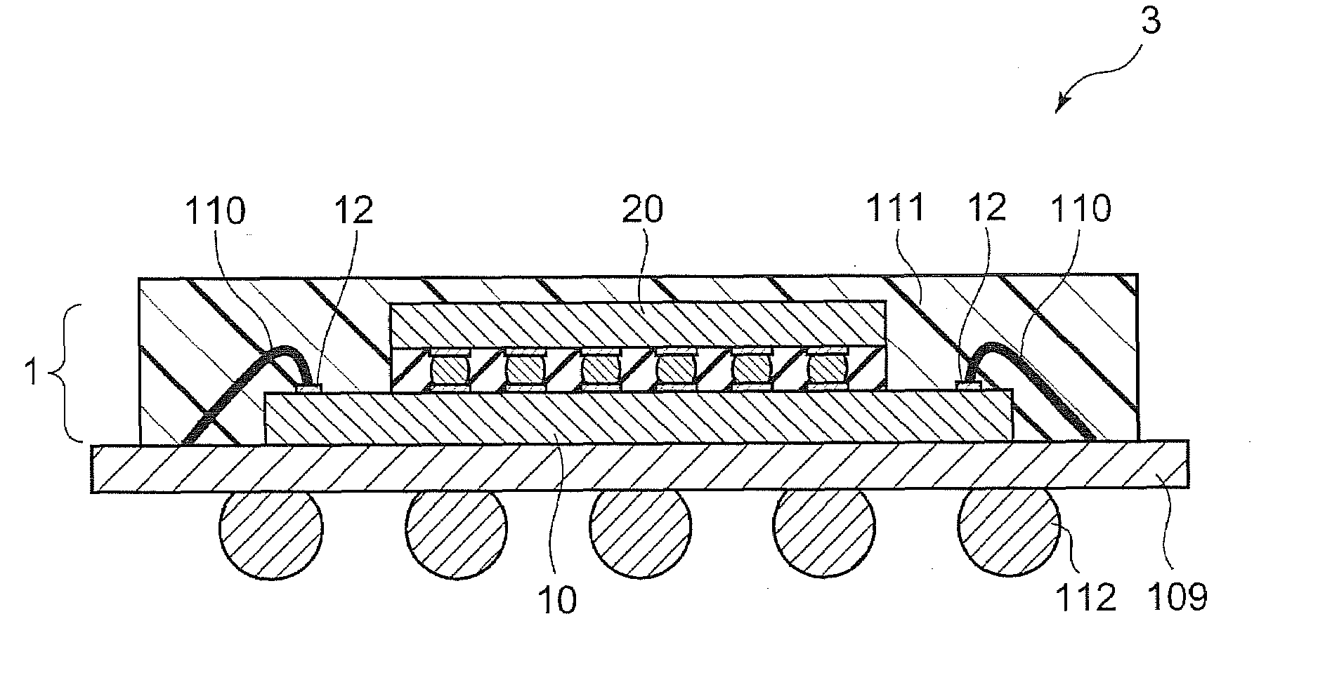
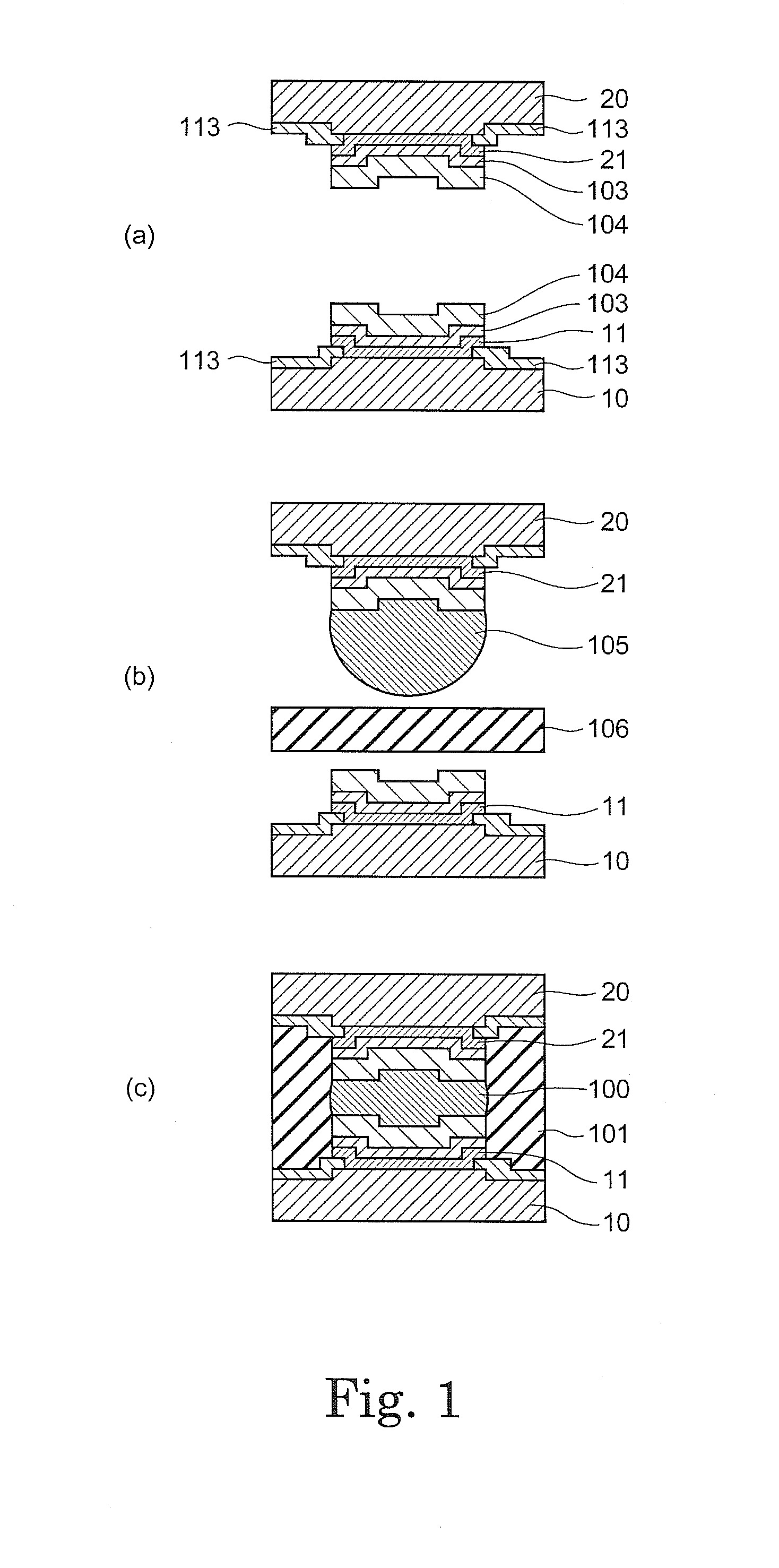
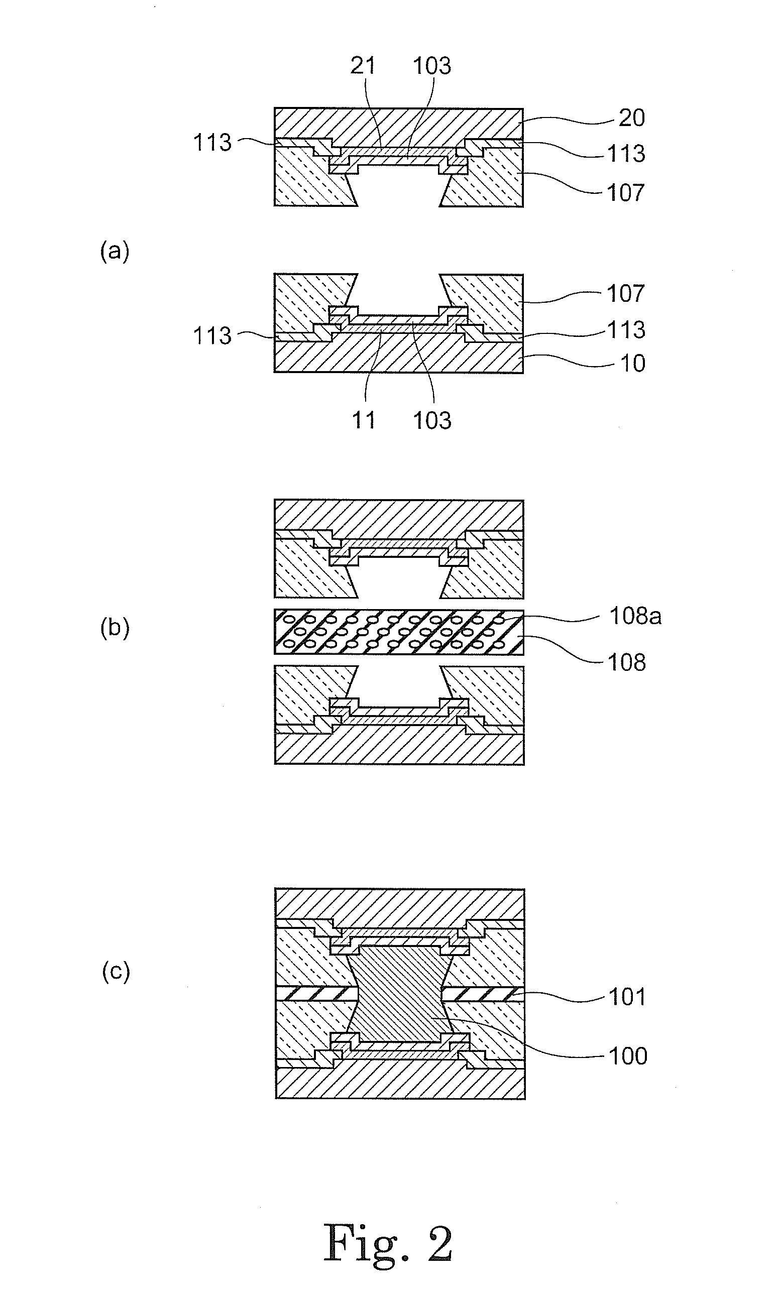
[0052]The adhesive tape according to the first embodiment of the present invention comprises: (A) a film forming resin; (B) a curable resin; and (C) a curing agent having flux activity at a predetermined blending ratio. The adhesive tape according to the first embodiment of the present invention is particularly suitably used in the case where electrical connection between semiconductor chips in a chip-on-chip type semiconductor device in which one semiconductor chip is mounted on another semiconductor chip face down is carried out using a flip-chip method. The adhesive tape of this embodiment is interposed between semiconductor chips opposed to each other to be subjected to thermal fusion, and thereby an oxidized film on the solder component constituting the solder bump which is formed on the opposed surface side of at least one of the semicondu...
second embodiment
b. Second Embodiment
[0113]Next, the adhesive tape according to the second embodiment of the present invention will be described.
[0114]The adhesive tape according to the second embodiment of the present invention further comprises (E) solder powder in addition to (A) a film forming resin, (B) a curable resin and (C) a curing agent having flux activity at a predetermined ratio. The adhesive tape according to the second embodiment of the present invention is particularly suitably used in the case where electrical connection between semiconductor chips in a chip-on-chip type semiconductor device in which one semiconductor chip is mounted on another semiconductor chip face down is performed utilizing self-alignment of the solder powder contained in the adhesive tape. The adhesive tape of this embodiment is interposed between the semiconductor chips opposed to each other and subjected to thermal fusion, and thereby the solder powder contained in the adhesive tape is aggregated between the...
examples
[0150]Hereinafter, the present invention will be specifically described by way of illustrative examples, but the present invention is not limited thereto.
1. Preparation of Adhesive Tape
[0151]Examples of blending amounts and preparation methods for the adhesive tape of the present invention are shown in Examples 1 to 23. Examples 1 to 10, 20 and 21 correspond to the adhesive tape of the second embodiment of the present invention, and Examples 11 to 19, 22 and 23 correspond to the adhesive tape of the first embodiment of the present invention. Further, Comparative Examples 1 and 2 are provided for comparison with Examples 1 to 10, 20 and 21, and Comparative Examples 3 and 4 are provided for comparison with Examples 11 to 19, 22 and 23.
Examples 1 to 10, 20 and 21
[0152]Components were mixed with acetone employing the blending amounts described in Table 1 in a manner in which the solid content was 40 wt %. Each varnish thus obtained was applied on a polyester sheet subjected to antistati...
PUM
| Property | Measurement | Unit |
|---|---|---|
| temperature | aaaaa | aaaaa |
| diameter | aaaaa | aaaaa |
| melt viscosity | aaaaa | aaaaa |
Abstract
Description
Claims
Application Information