Semiconductor Device

Inactive Publication Date: 2010-04-01
SEMICON ENERGY LAB CO LTD
View PDF27 Cites 19 Cited by
  • Summary
  • Abstract
  • Description
  • Claims
  • Application Information

AI Technical Summary

Benefits of technology

[0019]An RF tag having a protection circuit according to one embodiment of the present invention can protect an internal element from high power which is received by the RF tag even when the communication distance is extremely short. Therefore, improvement in reliability of the RF tag can be achieved. In addition, the protection circuit according to the above embodiment of the present invention

Problems solved by technology

Since the operation of a protection circuit is similar to the operation of a modulation circuit using a load modulation method (which is provided in an RF tag), a signal which is transmitted from the RF tag to a reader/writer is adversely affected in no small measure.

Method used


Image

  • Semiconductor Device
  • Semiconductor Device
  • Semiconductor Device

Examples


embodiment 1

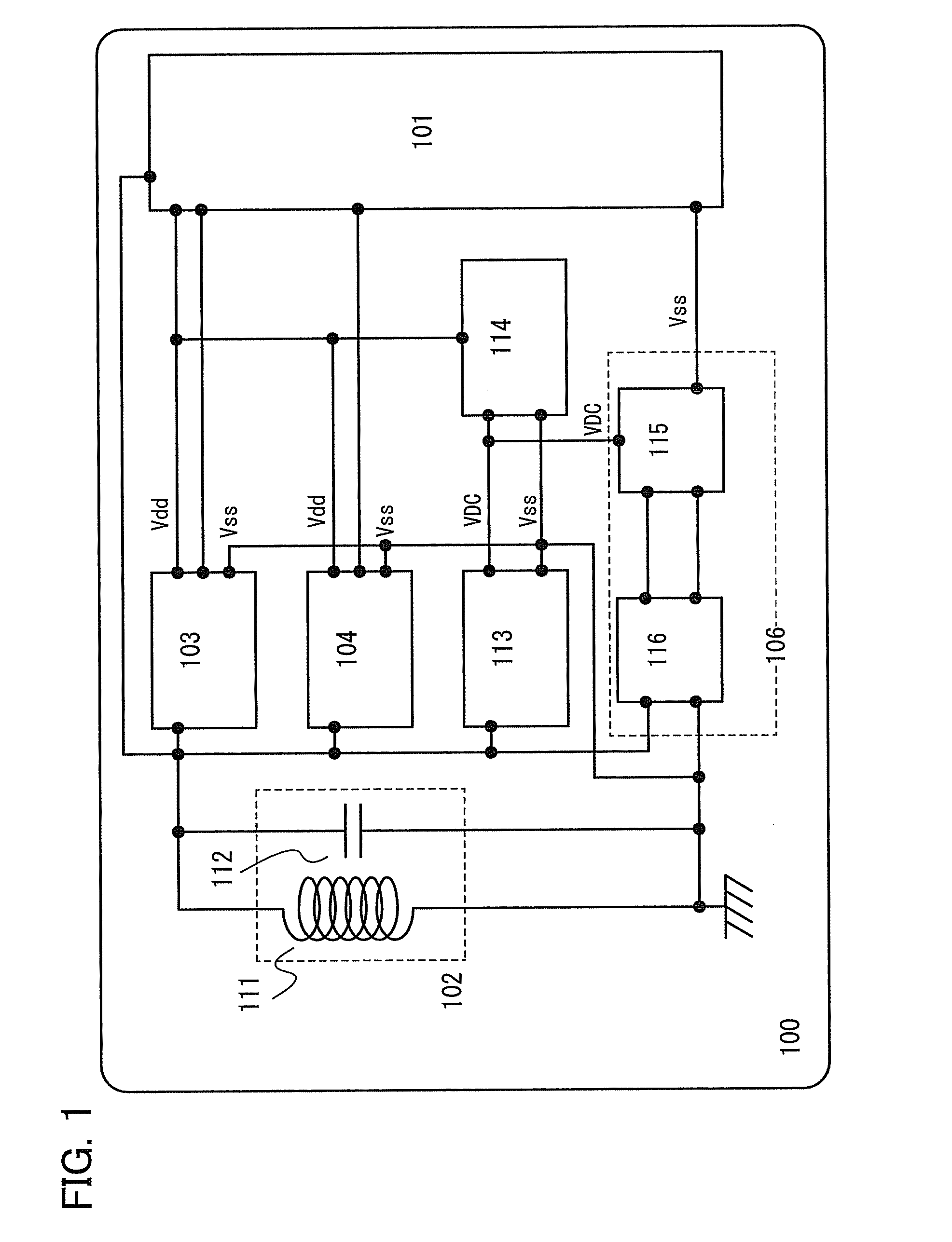
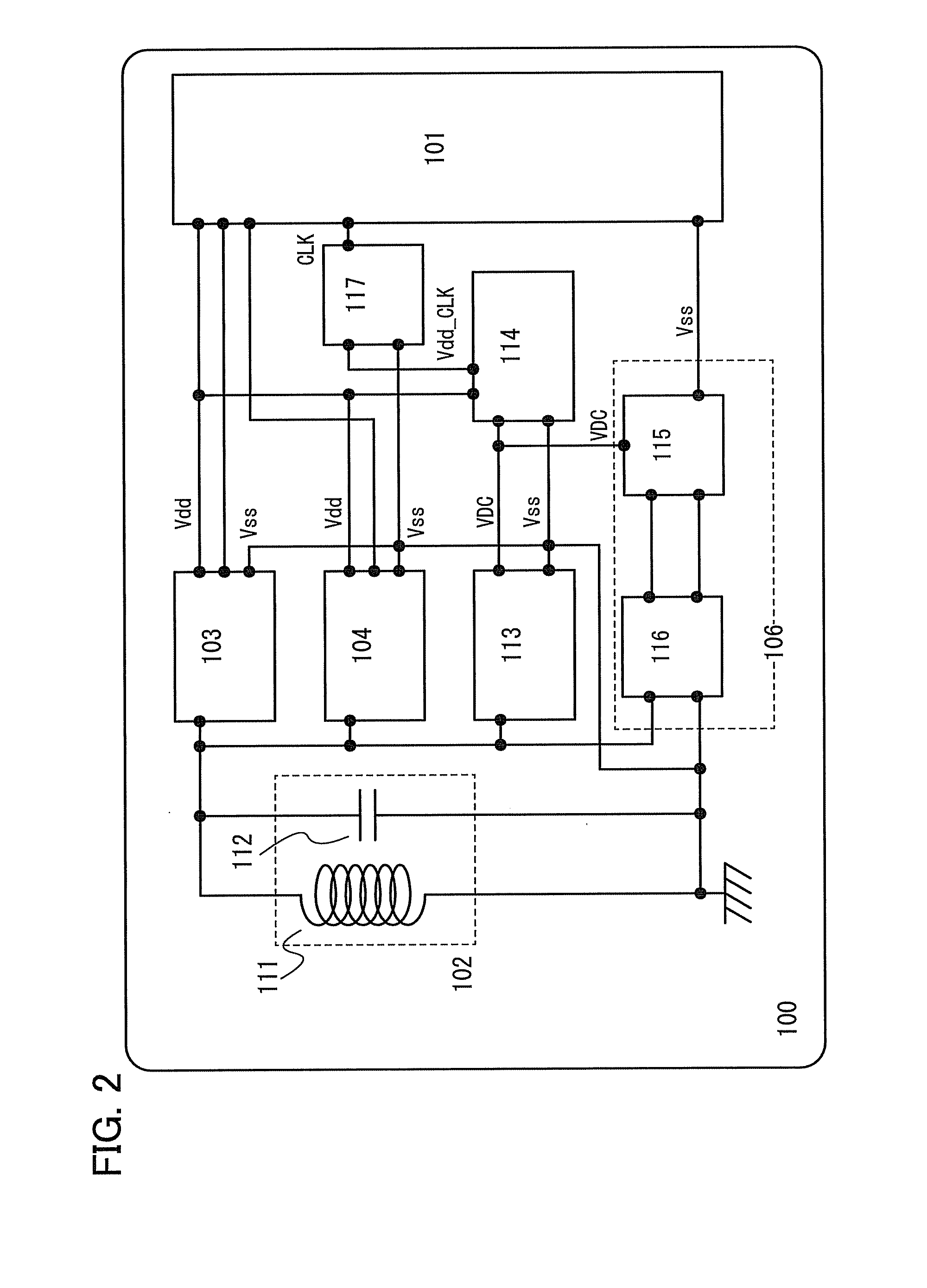
[0034]FIG. 1 shows a block diagram of the whole RF tag which is used as one embodiment of the present invention. An RF tag 100 includes the following: a logic circuit 101 for performing functional processing such as generation of a response signal based on received data; an antenna circuit 102 for transmitting and receiving (communicating) a signal between a reader / writer and the RF tag; a demodulation circuit 103 for demodulating an amplitude modulation wave (generated by superimposing a modulation wave on a carrier wave) which is received in the antenna circuit 102 and for extracting a pulse signal; a modulation circuit 104 for modulating a carrier wave outputted from the reader / writer in accordance with a response signal outputted from the logic circuit 101 and for transmitting a response signal to the reader / writer; a rectifier circuit 113 for generating DC voltage from the carrier wave or amplitude modulation wave which is received in the antenna circuit 102; and a protection c...

embodiment 2

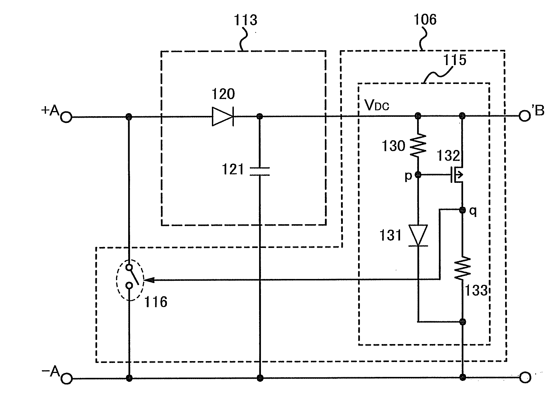
[0043]In this embodiment, the configuration and operation of the rectifier circuit and protection circuit which are described in Embodiment 1 will be described. FIG. 3 shows an example of a circuit configuration of a rectifier circuit and a protection circuit according to one embodiment of the present invention.

[0044]The rectifier circuit 113 includes a diode 120 and a capacitor 121. An anode of the diode 120 is electrically connected to one end of the antenna (in FIG. 3, electrically connected to a +A terminal side), and a cathode of the diode 120 is electrically connected to one electrode of the capacitor 121. In addition, the other electrode of the capacitor 121 is electrically connected to the other end of the antenna (in FIG. 3, electrically connected to a −A terminal side).

[0045]Note that since an antenna is a balanced device, a sine wave having a certain frequency is inputted into each of one end and the other end of the antenna in the RF tag. A signal of one end and a signal...

embodiment 3

[0064]A semiconductor device such as an RF tag includes a semiconductor integrated circuit which is formed using a plurality of minute semiconductor elements. A protection circuit according to one embodiment of the present invention is also formed using a semiconductor element. Therefore, malfunction of a circuit or damage of a semiconductor element due to electrostatic discharge (ESD) from the outside is likely to be caused. In particular, there is a high possibility that electrostatic discharge is caused to an RF tag having an antenna which is a conductor having a large surface area. In this embodiment, an example of a structure for protecting the semiconductor integrated circuit from such electrostatic discharge will be described.

[0065]Structural examples are shown in FIGS. 11A to 11D. In this embodiment, a semiconductor integrated circuit can be protected by providing a shielding body having a conductive material in the vicinity of the semiconductor integrated circuit. Note that...


PUM


Abstract

To provide a highly reliable semiconductor device (an RF tag) which operates normally even when a communication distance is extremely short, a protection circuit (a limiter circuit) for protecting an element which forms a semiconductor device (an RF tag) capable of wirelessly communicating data is provided. When the DC power supply potential which is generated in a rectifier circuit is equal to or greater than a predetermined value (a reference value), the protection circuit is made to operate, and the value of the generated DC power supply potential is reduced. On the other hand, when the DC power supply potential which is generated in the rectifier circuit is equal to or less than the predetermined value (reference value), the protection circuit is made not to operate, and the value of the generated DC power supply potential is used without change.

Description

TECHNICAL FIELD[0001]The present invention which is disclosed in this specification relates to a semiconductor device (a data carrier) capable of communicating (transmitting and receiving) data wirelessly. In particular, the present invention relates to a protection circuit which prevents breakage or deterioration of elements which are included in a semiconductor device when the semiconductor device receives high power in wireless communication.BACKGROUND ART[0002]In recent years, identification technology by which an ID number (identification number) is assigned to an individual object to clarify the history of information thereof, which is utilized for production, management, or the like, has attracted attention. In particular, an RFID (radio frequency identification) technique that transmits and receives data by wireless communication has been widely used. A wireless communication system using the RFID technique is a communication system including a wireless communication device ...

Claims


Application Information

Patent Timeline
IPC IPC(8): H02H9/00
CPCG06K19/0701G06K19/0715H01Q1/50H01Q1/2208G06K19/0723
Inventor FUJITA, MASASHI
Owner SEMICON ENERGY LAB CO LTD
Why Eureka
Try Eureka