Semiconductor laser device

a laser device and semiconductor technology, applied in semiconductor lasers, laser optical resonator construction, laser details, etc., can solve the problems of increasing the current required for laser oscillation, increasing the oscillation threshold value, and burdening the step of forming a multi-layer dielectric film, etc., to achieve the effect of suppressing the complications of manufacturing steps

Inactive Publication Date: 2010-04-01
SHARP KK
View PDF10 Cites 5 Cited by
  • Summary
  • Abstract
  • Description
  • Claims
  • Application Information

AI Technical Summary

Benefits of technology

[0027]An object of the present invention is to provide a semiconductor laser device capable of implem...

Problems solved by technology

If a stripe width is large, optical confinement in a lateral direction becomes unstable, resulting in a kink.
The increase in area of the current path causes an increase in current required for laser oscillation, and inevitably causes an increase in oscillation threshold value.
In the case of the conventional taper structures as in FIGS. 17 and 18, however, various disadvantages occur in a manufacturing process.
As shown in FIG. 20, however, the emitting surface sides are no...

Method used


Image

  • Semiconductor laser device
  • Semiconductor laser device
  • Semiconductor laser device

Examples


first embodiment

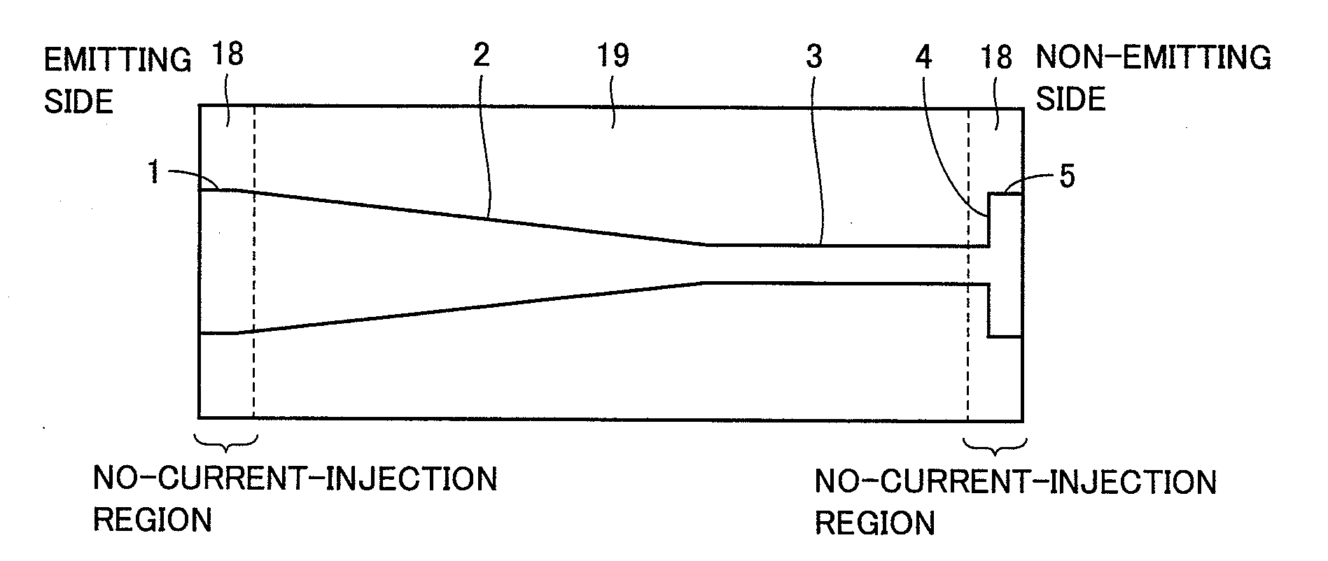
[0062]FIG. 2 is a cross-sectional view showing a cross section of window region 18 in the semiconductor laser device according to the first embodiment of the present invention. FIG. 3 is a cross-sectional view showing a cross section of internal region 19 in the semiconductor laser device.

[0063]As shown in FIGS. 2 and 3, the semiconductor laser device according to the present embodiment has a structure of stacked layers successively formed above an n-type GaAs substrate 11, the stacked-layer structure at least including: an n-type AlGaInP cladding layer 12; a multiple quantum well active layer 13 including a non-doped AlGaInP optical guide layer, a non-doped GaInP well layer, and a non-doped AlGaInP barrier layer; a p-type AlGaInP cladding layer 14; a p-type GaInP discontinuous band relaxing layer 15; and a p-type GaAs cap layer 16. In window region 18 (FIG. 2) provided in proximity to a facet of the resonator, zinc (Zn) is diffused to thereby disorder multiple quantum well active l...

second embodiment

[0083]FIGS. 12A and 12B are schematic diagrams each showing a cross section of a semiconductor laser device according to a second embodiment. FIG. 12A shows a cross section of internal region 19, while FIG. 12B shows a cross section of window region 18.

[0084]The semiconductor laser device is a modification of the semiconductor laser device according to the first embodiment, characterized in that the multiple quantum well active layer includes GaAs and AlGaAs, and that the semiconductor laser device is a high-power infrared laser device for a CD-R, having an oscillation wavelength in a 780 nm band.

[0085]With reference to FIGS. 12A and 12B, the semiconductor laser device according to the present embodiment has a structure of stacked layers successively formed above an n-type GaAs substrate 21. The stacked-layer structure is made of at least an n-type AlGaInP cladding layer 22, a multiple quantum well active layer 23 including a non-doped AlGaAs optical guide layer, a non-doped GaAs we...

third embodiment

[0092]FIGS. 13A and 13B are schematic diagrams each showing a cross section of a semiconductor laser device according to a third embodiment. FIG. 13A shows a cross section of internal region 19, while FIG. 13B shows a cross section of window region 18.

[0093]This semiconductor laser device is a modification of the semiconductor laser devices according to the first and second embodiments, characterized in that the structure of the multiple quantum well active layer includes GaN and InGaN, and that the semiconductor laser device is a high-power infrared laser device for a BD, having an oscillation wavelength in a 405 nm band.

[0094]With reference to FIGS. 13A and 13B, the semiconductor laser device according to the present embodiment has a structure of stacked layers successively formed above an n-type GaN substrate 31. The stacked-layer structure is made of at least an n-type AlGaN cladding layer 32, a multiple quantum well active layer 33 including a GaN optical guide layer, an InGaN ...


PUM


Abstract

A resonator in a semiconductor laser device includes a semiconductor substrate, an n-type cladding layer and a p-type cladding layer formed on or above the semiconductor substrate, and an active layer sandwiched between the n-type cladding layer and the p-type cladding layer. A ridge extending in an axial direction of the resonator is formed at an upper surface of the resonator. The ridge includes an emitting-side end portion, a non-emitting-side end portion, a taper portion allowing a width of the ridge to be decreased in a taper-like manner from the emitting-side end portion toward the non-emitting-side end portion, and a step portion provided on a side of the emitting-side end portion with respect to the non-emitting-side end portion, and allowing the width of the ridge to be changed in a step-like manner.

Description

[0001]This nonprovisional application is based on Japanese Patent Application No. 2008-250462 filed on Sep. 29, 2008, with the Japan Patent Office, the entire contents of which are hereby incorporated by reference.BACKGROUND OF THE INVENTION[0002]1. Field of the Invention[0003]The present invention relates to a semiconductor laser device, and particularly relates to a semiconductor laser device used for an optical pickup device and others.[0004]2. Description of the Background Art[0005]In recent years, a recording speed has been improved in an optical pickup device. For example, a CD-R, a DVD-R / RW, and others that have achieved a 16× recording speed have been commercialized. To increase the recording speed, the semiconductor laser device is required to achieve high power.[0006]To allow the semiconductor laser device to achieve high power, there is a demand for: a high COD (Catastrophic Optical Damage) level, namely, a high optical power limitation determined by a COD; linearity in c...

Claims


Application Information

Patent Timeline
IPC IPC(8): H01S5/323H01S5/00
CPCB82Y20/00H01S5/0655H01S5/10H01S5/1039H01S5/34326H01S5/16H01S5/162H01S5/32341H01S5/1064
Inventor SUGAHARA, AKIYOSHI
Owner SHARP KK
Why Eureka
Try Eureka