

Method for producing group III nitride compound semiconductor element
a technology of nitride and compound semiconductor elements, which is applied in the direction of semiconductor devices, basic electric elements, electrical appliances, etc., can solve the problems of high load stress, poor yield, and large volume expansion in the decomposed area, and achieves less deterioration of element characteristics and high yield
- Summary
- Abstract
- Description
- Claims
- Application Information
AI Technical Summary
Benefits of technology
Problems solved by technology
Method used
Image

Examples
example 1
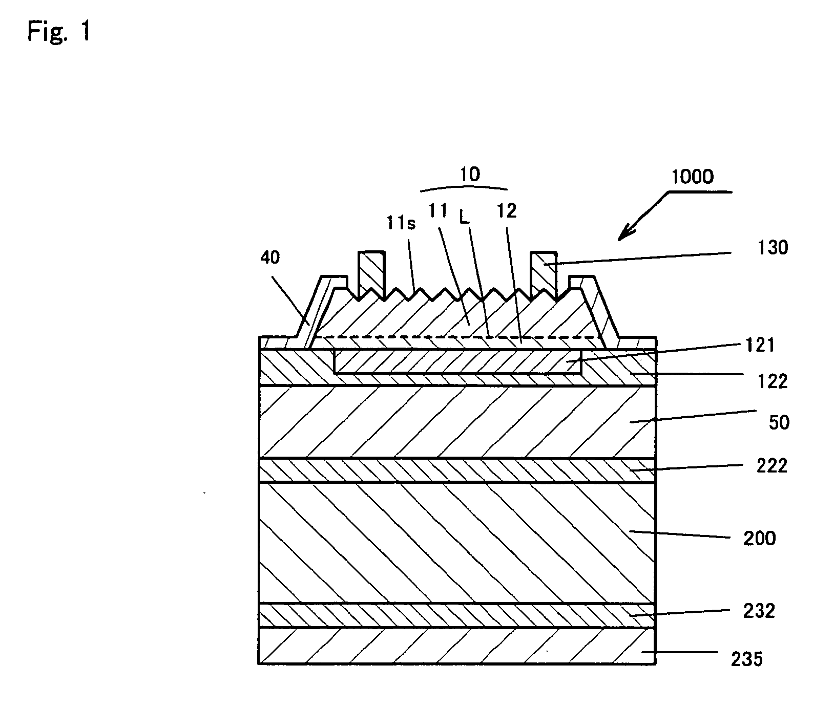
[0124]FIG. 1 is a cross sectional view illustrating the structure of a Group III nitride compound semiconductor element (Blue LED) obtained by a production method according to one specific Example of the invention.
[0125]The Group III nitride compound semiconductor element (Blue LED) 1000 of FIG. 1 has a laminated structure containing a conductive layer 222 containing a laminate of a plurality of metals, a solder layer 50 which is a low melting point alloy layer, a conductive layer 122 containing a laminate of a plurality of metals, a p contact electrode 121, a p type layer 12 containing a single layer or a multilayer of mainly a p type Group III nitride compound semiconductor layer, a light emitting region L, an n type layer 11 containing a single layer or a multilayer of mainly an n type Group III nitride compound semiconductor layer, and an n contact electrode 130 from the side of the supporting substrate 200 on the surface of a conductive supporting substrate 200 serving as a p t...
example 2
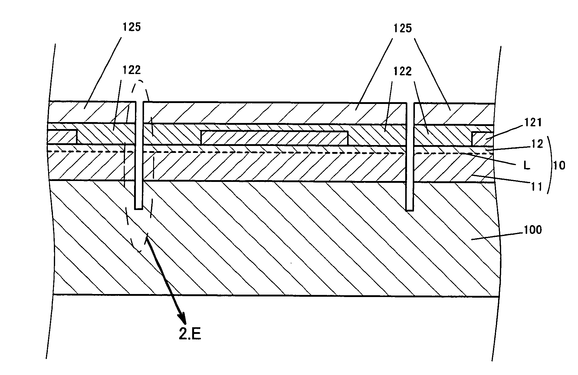
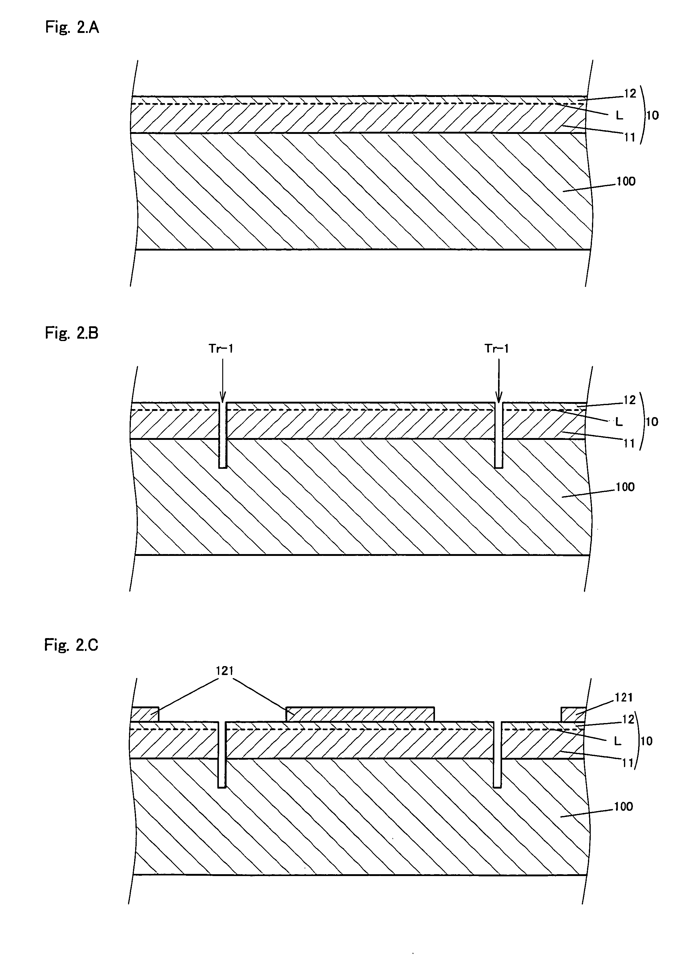
[0157]In Example 1, the second grooves tr-2 were formed so that the first grooves tr-1 were present in the area as illustrated in FIG. 2.J which is a flow chart and FIG. 2.K which is an enlarged view of the vicinity of the first grooves. In this case, the side surfaces of the epitaxial layer 10 forming the first grooves tr-1 were also removed.
[0158]However, the second grooves tr-2 may be formed so that the first grooves tr-1 are not present in the area. More specifically, the second grooves tr-2 were formed while leaving the side surfaces of the epitaxial layer 10 forming the first grooves tr-1, and the first grooves tr-1 may be removed in the process of cutting the supporting substrate 200. This method is defined as Example 2 and will be described using FIGS. 3.A and 3.B.
[0159]FIG. 3.A is an enlarged view illustrating the vicinity of the first grooves tr-1 and the second grooves tr-2 after the second grooves tr-2 were formed by the production method of this Example.
[0160]In Example...
modified example
[0165]In a supporting substrate cutting process, laser irradiation for cutting (separation) may be carried out several times at a plurality of portions. For example, as illustrated in FIG. 4, a plurality of dashed line oval inner areas were decomposed or melted by laser irradiation. The substrate may be cut with a wider width by changing the laser irradiation position.
[0166]As an advantage of this technique, omitting of the thinning of the supporting substrate 200 prior to the supporting substrate cutting process of Example 1 is mentioned. Or, when the formation of the first grooves carried out by a dicer in Example 1 was carried out by laser irradiation, the laser irradiation in the supporting substrate cutting process can be carried out while adjusting the focusing degree and the output to be the same as those in the formation of the first grooves.
PUM
| Property | Measurement | Unit |
|---|---|---|
| depth | aaaaa | aaaaa |
| thickness | aaaaa | aaaaa |
| thickness | aaaaa | aaaaa |
Abstract
Description
Claims
Application Information