Backside Connection to TSVs Having Redistribution Lines

Active Publication Date: 2010-04-15
TAIWAN SEMICON MFG CO LTD
View PDF6 Cites 98 Cited by
  • Summary
  • Abstract
  • Description
  • Claims
  • Application Information

AI Technical Summary

Benefits of technology

[0010]The advantageous features of the present invention include

Problems solved by technology

Although dramatic improvements in lithography have resulted in considerable improvements in 2D integrated circuit formation, there are physical limitations to the density that can be achieved in two dimensions.
One of these limitations is the minimum size needed to make these components.
Also, when more devices are put into one chip, more

Method used


Image

  • Backside Connection to TSVs Having Redistribution Lines
  • Backside Connection to TSVs Having Redistribution Lines
  • Backside Connection to TSVs Having Redistribution Lines

Examples


Embodiment Construction

[0014]The making and using of the embodiments of the present invention are discussed in detail below. It should be appreciated, however, that the embodiments of the present invention provide many applicable inventive concepts that can be embodied in a wide variety of specific contexts. The specific embodiments discussed are merely illustrative of specific ways to make and use the invention, and do not limit the scope of the invention.

[0015]A novel backside connection structure connecting to through-silicon vias (TSVs) and the method of forming the same are provided. The intermediate stages of manufacturing a preferred embodiment of the present invention are illustrated. The variations of the preferred embodiments are discussed. Throughout the various views and illustrative embodiments of the present invention, like reference numbers are used to designate like elements.

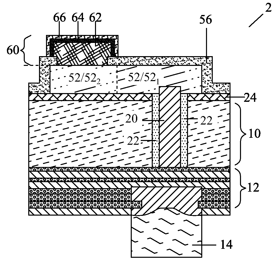
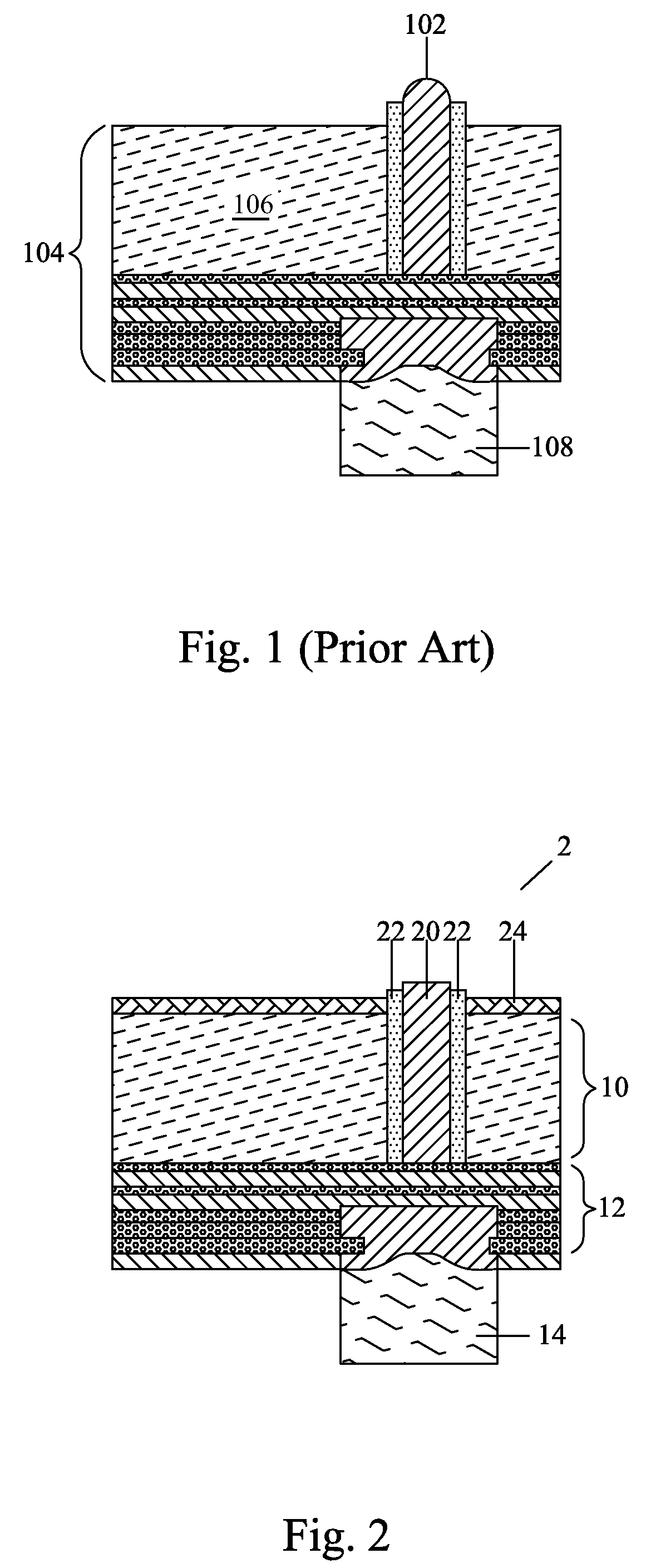
[0016]Referring to FIG. 2, chip 2, which includes substrate 10 and integrated circuits (not shown) therein, is provi...


PUM


Abstract

An integrated circuit structure includes a semiconductor substrate including a front side and a backside. A through-silicon via (TSV) penetrates the semiconductor substrate, and has a back end extending to the backside of the semiconductor substrate. A redistribution line (RDL) is over the backside of the semiconductor substrate and connected to the back end of the TSV. The integrated circuit structure further includes a passivation layer over the RDL; an opening in the passivation layer, wherein a portion of the RDL is exposed through the opening; and a nickel layer in the opening and contacting the RDL.

Description

[0001]This application claims the benefit of U.S. Provisional Patent Application Ser. No. 61 / 104,172, filed Oct. 9, 2008, and entitled “Formation Scheme for TSV Backside RDL and Pad,” which application is hereby incorporated herein by reference.TECHNICAL FIELD[0002]This invention relates generally to integrated circuit structures, and more particularly to through-silicon vias, and even more preferably to the formation of bond pads connected to the through-silicon vias.BACKGROUND[0003]Since the invention of integrated circuits, the semiconductor industry has experienced continuous rapid growth due to constant improvements in the integration density of various electronic components (i.e., transistors, diodes, resistors, capacitors, etc.). For the most part, this improvement in integration density has come from repeated reductions in minimum feature size, allowing more components to be integrated into a given chip area.[0004]These integration improvements are essentially two-dimensiona...

Claims


Application Information

Patent Timeline
IPC IPC(8): H01L23/538
CPCH01L21/76898H01L24/03H01L2924/01327H01L2924/01047H01L2924/01023H01L2924/00013H01L2224/0558H01L2924/19043H01L2924/19041H01L2924/14H01L2924/014H01L2924/01322H01L2924/01082H01L2924/01079H01L2924/01078H01L24/05H01L24/06H01L2224/0401H01L2224/05155H01L2224/05164H01L2224/05552H01L2224/05568H01L2224/0557H01L2224/05644H01L2224/13155H01L2224/13582H01L2224/13644H01L2224/13664H01L2224/16H01L2924/01013H01L2924/01014H01L2924/01029H01L2924/01033H01L2924/01046H01L2924/0105H01L2924/00014H01L2224/13099H01L2924/00012H01L2224/023H01L2924/0001
Inventor HSU, KUO-CHINGCHEN, CHEN-SHIEN
Owner TAIWAN SEMICON MFG CO LTD
Why Eureka
Try Eureka